

Exhibition Invitation丨Pengcheng Semiconductor sincerely invites you to attend the 2025 China Materials Congress!
Release time:
2025-07-01


I. Conference Introduction
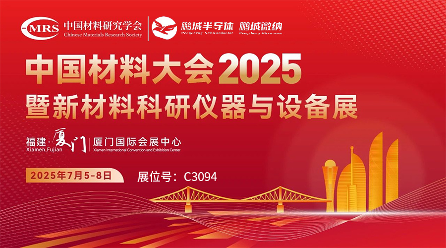
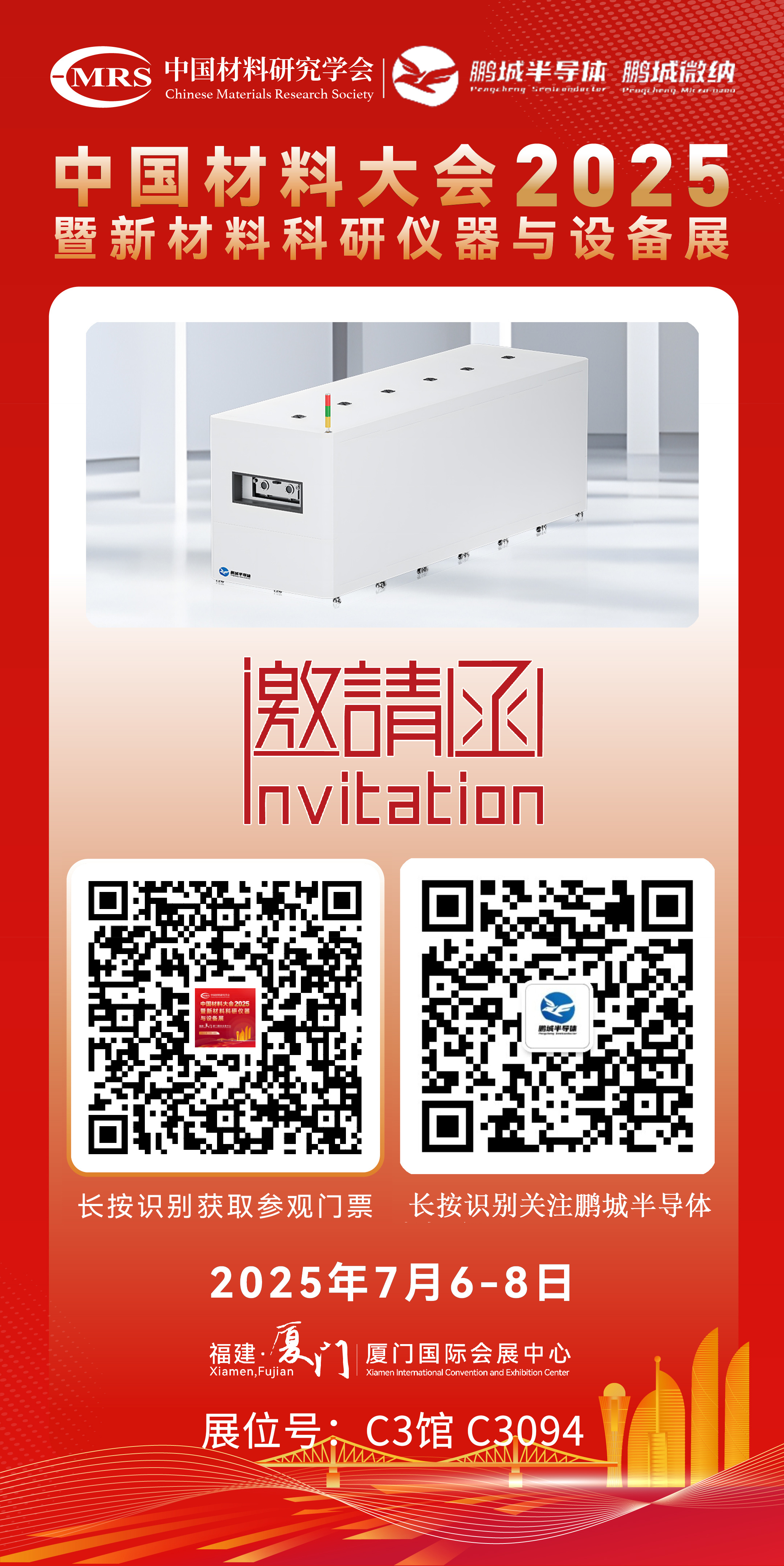
The "China Materials Congress 2025" will be held at the Xiamen International Convention and Exhibition Center in Fujian Province from July 5th to 8th, 2025. The conference is expected to attract 30,000 participants and will feature approximately 115 domestic and international sub-conferences covering five major themes: energy materials, environmental materials, advanced structural materials, functional materials, and material design, preparation, and evaluation. A series of special forums will also be held, including a youth forum, a special new materials forum, a materials education forum, and a materials journal forum. In addition, an international new materials scientific research instrument and equipment exhibition will be held concurrently.
II. Booth Information
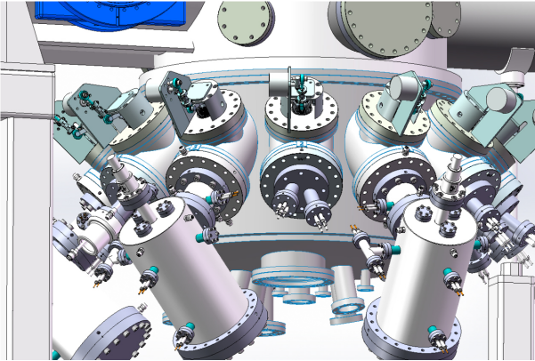
Pengcheng Semiconductor Will bring technology based on nano and atomic manufacturing PVD/CVD for high-quality thin film preparation. For example, using magnetron sputtering technology for single-crystal thin film preparation, and using magnetron sputtering as a beam source for molecular beam epitaxy. Booth number: Hall C3, Booth C3094. Welcome to visit and exchange technology.
III. Featured Products
* Single-crystal thin film preparation using magnetron sputtering technology, and using magnetron sputtering as a beam source for molecular beam epitaxy
* Magnetron sputtering technology solves the problem of micro-hole coating with an aspect ratio higher than 10:1
* Large-size polycrystalline diamond wafers for use as heat sinks for high-power devices, high-frequency devices, and high-power lasers
* Using single-frequency or dual-frequency plasma-enhanced chemical vapor deposition technology, it is an ideal process equipment for depositing high-quality silicon nitride and silicon oxide thin films
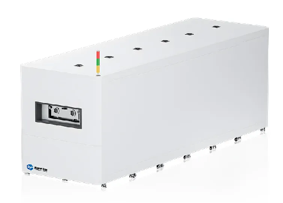
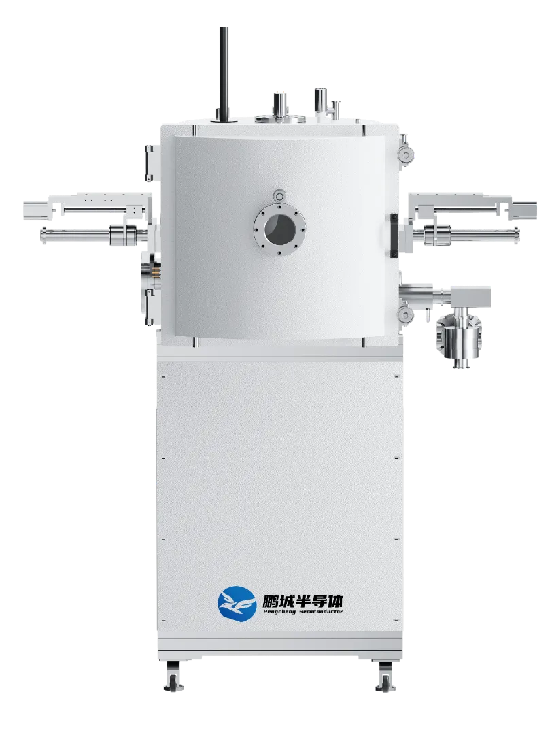
Molecular Beam Epitaxy (MBE) thin film growth equipment

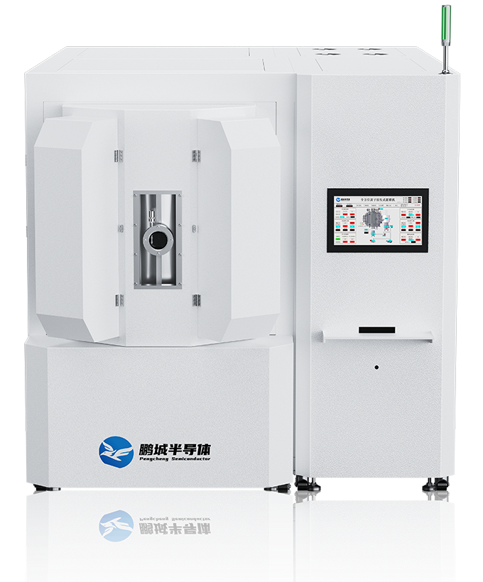
Production-type TGV/TSV/TMV high-vacuum magnetron sputtering coating machine
Production-type high-vacuum magnetron sputtering/ion-assisted/multi-arc composite coating machine
Production-type high-vacuum magnetron sputtering and ion-assisted composite coating machine
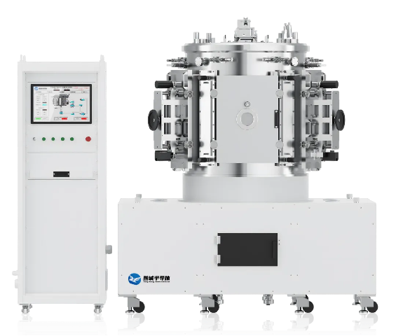
Research-type high-vacuum magnetron sputtering coating machine
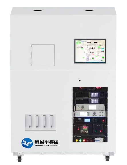
HFCVD hot-wire chemical vapor deposition equipment
PECVD plasma-enhanced chemical vapor deposition equipment
IV. Pengcheng Semiconductor Technology (Shenzhen) Co., Ltd.
Pengcheng Semiconductor Technology (Shenzhen) Co., Ltd. was jointly founded by Harbin Institute of Technology (Shenzhen) and a team of engineers with many years of practical experience. The company is committed to innovation and sustainable development, addressing industry pain points and localization challenges, and striving for independent and controllable industrial chains.
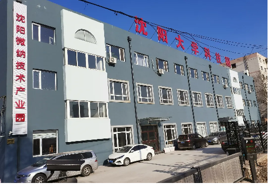
Pengcheng Micro-Nano Technology (Shenyang) Co., Ltd. is a wholly-owned subsidiary of Pengcheng Semiconductor Technology (Shenzhen) Co., Ltd., serving as the design center and production base for semiconductor processes and equipment.
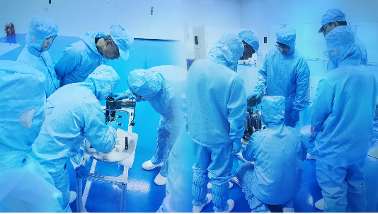
The company's core business is micro-nano technology and high-end precision manufacturing, with specific applications including the R&D, design, production, manufacturing, and process technology services of semiconductor materials, semiconductor processes, and semiconductor equipment, as well as the upgrading and transformation of semiconductor equipment. It can provide process R&D and prototyping services for users.
The company's talent team has a complete knowledge structure, with a high-level materials research and process research team led by professors and doctors from Harbin Institute of Technology; and a senior equipment designer team from the industry, with over 20 years of experience in semiconductor materials research, epitaxial technology research, and the design, production, and manufacturing of complete sets of semiconductor thin film preparation equipment.
Relying on Harbin Institute of Technology (Shenzhen), the company has advanced semiconductor R&D equipment platforms and testing equipment platforms, enabling it to conduct research at a high starting point. The company's headquarters is located in Shenzhen, with the ability to conduct R&D, production, debugging of semiconductor equipment, and pilot testing, production, and sales of semiconductor materials and devices.
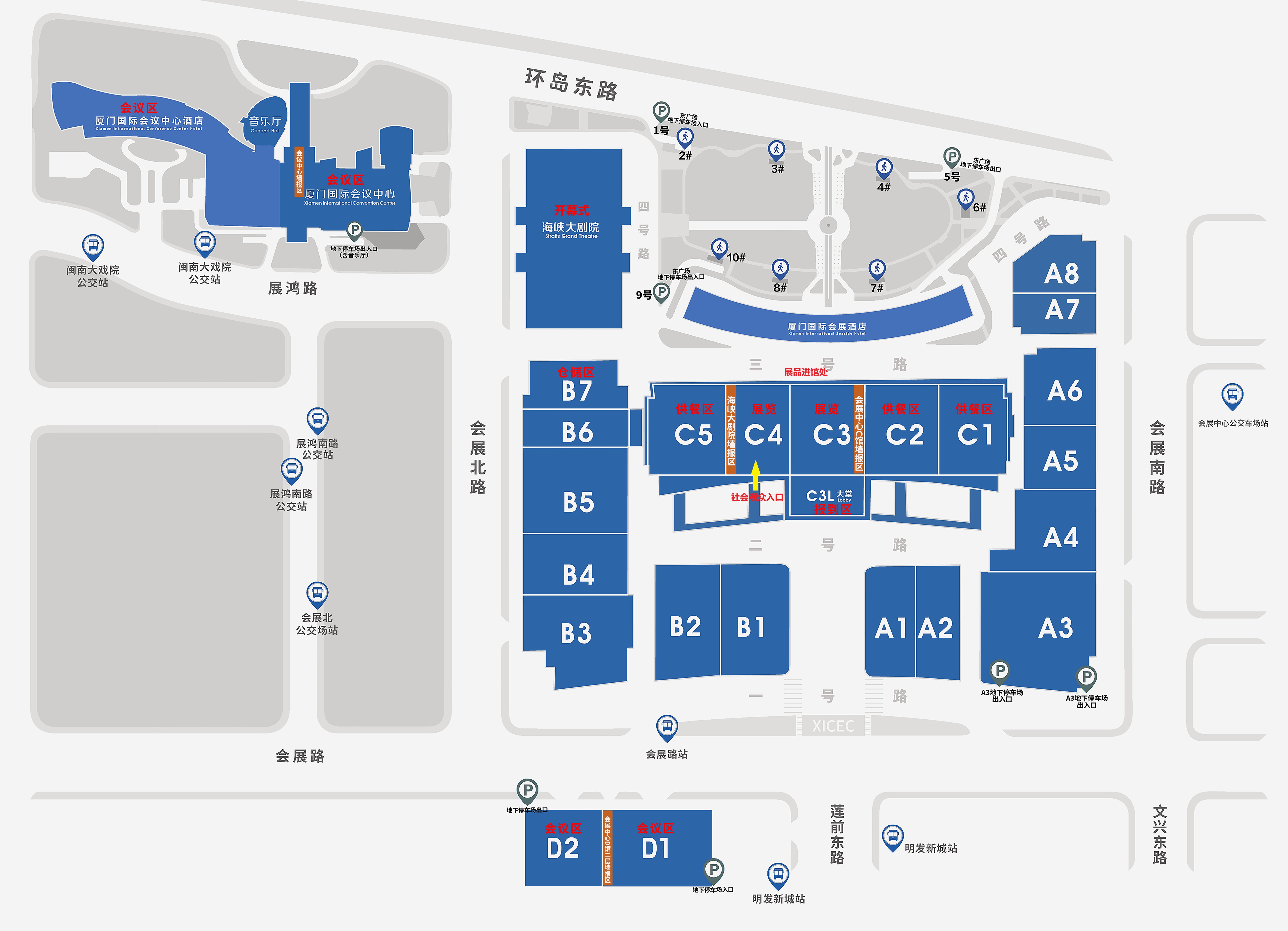
V. Convention Center Transportation Map

VI. Forum Activities

News Center
“The Coating Black Technology” Hidden in Medical Imaging

Contact: Miss Dai
Address: 1704, Building 1, Chongwen Park, Nanshan Zhiyuan, 3370 Liuxian Avenue, Nanshan District, Shenzhen City, Guangdong Province
Shenyang Office Address: Shenyang University Science Park, No.15 Wanghua South Street, Dadong District, Shenyang City, Liaoning Province
Telephone:13632750017
E-mail:sales@hitsemi.com

Message