Application of TGV Glass Through-Hole Technology in Magnetron Sputtering


Release time:

2026-01-05

As an advanced micro- and nano-fabrication technique, TGV glass via-hole technology has demonstrated tremendous application potential in the field of magnetron sputtering. By precisely fabricating vias on glass substrates, this technology not only enables vertical interconnections for three-dimensional circuits but also significantly enhances the integration and performance of electronic devices.

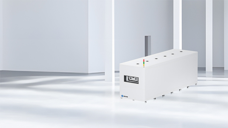
TGV glass through-hole As an advanced micro- and nano-fabrication technique, the technology... Magnetron sputtering This technology demonstrates tremendous application potential in various fields. By precisely fabricating through-holes on glass substrates, it not only enables vertical interconnections for three-dimensional circuits but also significantly enhances the integration and performance of electronic devices. During magnetron sputtering, TGV glass vias serve as conductive channels, guiding sputtered particles to deposit accurately in designated areas and forming high-quality, high-precision thin-film layers. This unique feature gives TGV glass via technology a distinct advantage in the fabrication of high-performance sensors, microelectromechanical systems (MEMS), and advanced optical components. Moreover, this technology boasts excellent thermal and chemical stability, ensuring long-term reliable operation even under harsh environmental conditions, thereby further expanding the scope of magnetron sputtering applications. As microelectronics technology continues to advance, the integration of TGV glass via technology with magnetron sputtering will become increasingly close. This synergy holds great promise for playing a pivotal role in cutting-edge fields such as integrated circuit packaging, 5G communications, and the Internet of Things, driving related industries toward higher levels of development.

News Center

The TGV glass through-hole technology has achieved a significant breakthrough, and its application prospects continue to expand.

Recently, TGV (Through Glass Via) technology has made significant strides in the fields of materials processing and micro- and nano-manufacturing, drawing considerable attention from the semiconductor, advanced packaging, and emerging electronic device industries. With its outstanding electrical performance, high-frequency characteristics, and three-dimensional integration capabilities, TGV is emerging as one of the key technologies for next-generation high-density interconnects.

Application of TGV Glass Through-Hole Technology in Magnetron Sputtering

As an advanced micro- and nano-fabrication technique, TGV glass via-hole technology has demonstrated tremendous application potential in the field of magnetron sputtering. By precisely fabricating vias on glass substrates, this technology not only enables vertical interconnections for three-dimensional circuits but also significantly enhances the integration and performance of electronic devices.

Diamond: Possessing potential that surpasses existing semiconductor materials, with broader application prospects in the future.

Diamond is used as a semiconductor material—and some scholars even hail it as the “ultimate semiconductor material” and the “ultimate room-temperature quantum material”—owing to its unique physical and chemical properties. Diamond is an ultra-wide-bandgap semiconductor that boasts exceptional electrical, optical, mechanical, thermal, and chemical characteristics. These properties give diamond broad application prospects in numerous fields.

Pengcheng Semiconductor: The Strategy, Tactics, and Survival Guide of a High-Tech Enterprise

The 15th China International Nanotechnology Industry Expo (referred to as "Nanobio"), held under much anticipation, successfully came to a close. This year's event featured one keynote speech, 15 parallel forums, and hosted 605 cutting-edge presentations. Additionally, it included an innovation and entrepreneurship competition, along with three supply-and-demand matchmaking sessions. The expo brought together over 150 nationally recognized talents and more than 500 top experts from leading universities, research institutions, and corporate organizations both domestically and internationally. With an exhibition area spanning 25,000 square meters, the event attracted over 350 of the world's premier companies and institutions, showcasing more than 2,400 of the latest nanotechnology products and innovative applications globally. Over the three-day period, the expo drew nearly 27,500 attendees in total, making it the largest-ever edition in terms of scale and cementing its growing influence on the global stage.

Pengcheng Semiconductor Debuts at the High-End Professional Exhibition on "Optoelectronics + Semiconductors"—Shenzhen's 26th China International Optoelectronic Exposition

When the "light-speed" innovation of optoelectronics meets the "subtle" breakthroughs in semiconductors, two premier, high-end professional exhibitions leading global industry collaboration are set to make a cross-industry debut, shining brightly in Shenzhen. On September 10, the 26th China International Optoelectronic Expo (CIOE China Optics Expo) and SEMI-e Shenzhen International Semiconductor Exhibition, along with the 2025 Integrated Circuit Industry Innovation Expo, unveiled themselves at the Shenzhen International Convention & Exhibition Center. With an exhibition space exceeding 300,000 square meters, attracting over 5,000 exhibitors and expected to draw 160,000 professional visitors, these events have established a new benchmark for collaborative development between the optoelectronics and semiconductor industries, injecting powerful momentum into the global tech sector as it breaks through technological barriers and sparks fresh waves of innovation.