

Diamond: Possessing potential that surpasses existing semiconductor materials, with broader application prospects in the future.
Release time:
2025-12-16


Diamond It is used as a semiconductor material and has even been hailed by some scholars as the “ultimate semiconductor material” and the “ultimate room-temperature quantum material,” owing to its unique physical and chemical properties. Diamond is an ultra-wide-bandgap semiconductor that boasts exceptional electrical, optical, mechanical, thermal, and chemical characteristics. These properties give diamond broad application prospects in numerous fields.
First, diamond possesses an extremely large bandgap, which is crucial for its use as a semiconductor material. Materials with large bandgaps can maintain excellent performance even in high-temperature environments—a advantage that other semiconductor materials find hard to match. In addition, diamond also boasts high thermal conductivity, high hole mobility, high dielectric strength, and a low dielectric constant.
Among these properties, the high thermal conductivity is particularly important for manufacturing high-power amplifiers. If chips are made from diamond, their high thermal conductivity can effectively dissipate the heat generated during operation, which is of great significance in alleviating the overheating problem that often occurs when using electronic devices such as mobile phones.
In addition, diamond possesses several advantageous properties, including high-pressure resistance, high radio-frequency performance, low cost, and excellent high-temperature tolerance, making it an ideal candidate for next-generation semiconductor materials. Compared to existing materials such as gallium nitride and silicon carbide, diamond has a wider bandgap and higher carrier mobility. At room temperature, diamond exhibits an extremely low intrinsic carrier concentration and boasts outstanding high-temperature performance.
In the past, diamonds were widely used—particularly in geological drilling and cutting operations—mainly because of their exceptional hardness and mechanical properties; they were even dubbed the “teeth of industry.” However, with advances in technology, the applications of diamonds are continually expanding. Currently, China is transitioning from a major producer of superhard materials to a global leader in this field, striving to enhance product quality and build internationally recognized brands. At the same time, diamond applications are increasingly shifting toward wear-resistant products, ultra-hard materials, and nanoscale applications, with particularly promising prospects in fields such as biomedicine.
Overall, diamond boasts broad application prospects in the semiconductor field thanks to its unique physical and chemical properties. In the future, as technology continues to advance, the applications of diamond will become even more extensive, and its importance in the semiconductor sector will continue to grow.
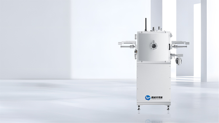
Hot-Wire CVD Diamond Film Deposition Equipment
Disclaimer:
This article is partially reprinted from the internet; copyright and responsibility for its content belong to the original author. If you are the original author and do not wish your work to be reprinted, please contact us at sales@hitsemi.com for assistance.
News Center
“The Coating Black Technology” Hidden in Medical Imaging

Contact: Miss Dai
Address: 1704, Building 1, Chongwen Park, Nanshan Zhiyuan, 3370 Liuxian Avenue, Nanshan District, Shenzhen City, Guangdong Province
Shenyang Office Address: Shenyang University Science Park, No.15 Wanghua South Street, Dadong District, Shenyang City, Liaoning Province
Telephone:13632750017
E-mail:sales@hitsemi.com

Message