

Pengcheng Semiconductor Debuts at the High-End Professional Exhibition on "Optoelectronics + Semiconductors"—Shenzhen's 26th China International Optoelectronic Exposition
Release time:
2025-09-17


When the "light-speed" innovation of optoelectronics meets the "subtle" breakthroughs in semiconductors, two premier, high-end professional exhibitions—leading global industry collaboration—are making a cross-industry debut and shining brightly in Shenzhen.
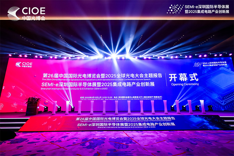
On September 10, the 26th China International Optoelectronics Expo (CIOE China Optoelectronics Expo) and SEMI-e Shenzhen International Semiconductor Exhibition, along with the 2025 Integrated Circuit Industry Innovation Expo, made their debut at the Shenzhen International Convention and Exhibition Center. With an exhibition area exceeding 300,000 square meters, the event brought together more than 5,000 exhibitors and is expected to attract 160,000 professional visitors, setting a new benchmark for the collaborative development of the "optoelectronics + semiconductor" industries. This landmark event is poised to inject powerful momentum into the global tech industry, helping break through technological barriers and reigniting innovation.
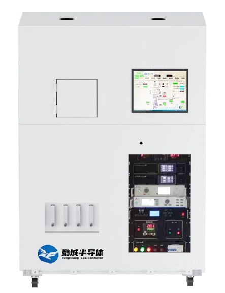
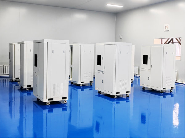
As a pioneering force in the semiconductor industry, Pengcheng Semiconductor Technology (Shenzhen) Co., Ltd. (Hereinafter referred to as “ Pengcheng Semiconductor "This time, we make a stunning debut with several core products developed entirely in-house, along with cutting-edge technologies rooted in nanotechnology and atomic manufacturing." PVD / CVD Technology for high-quality thin-film preparation. Used with Magnetron Sputtering The technology enables single-crystal thin-film preparation, utilizing magnetron sputtering for this purpose. Molecular Beam Epitaxy beam sources, and more. Utilizing magnetron sputtering technology to address aspect ratios exceeding 10:1 microporous coating 。
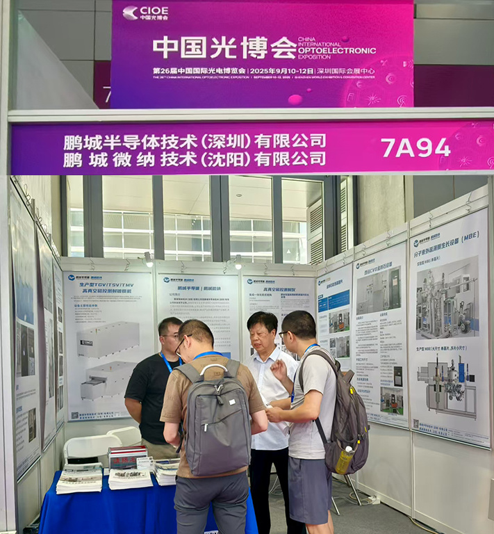
Production-grade TGV/TSV/TMV High-Vacuum Magnetron Sputtering Coating System Coating for high-density through-holes and blind vias on glass and ceramic substrates, with aspect ratios exceeding 10:1. For example, the process enables the deposition of Cu/Ti microstructures and Au/TiW dual-layer films for transmission lines on substrates, providing critical support for enhancing the integration density of microsystems.
Advantages: High uniformity and repeatability of the film layer, strong adhesion of the film, and equipment capable of programmable, automated control based on the process formula.
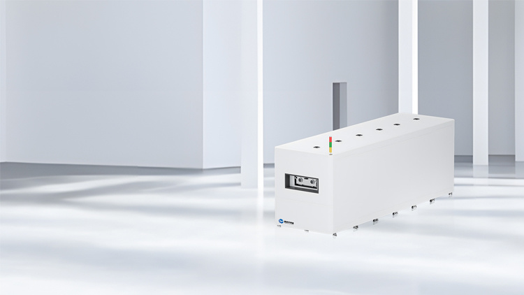
Hot-Wire Chemical Vapor Deposition HFCVD Equipment : It can be used to produce microcrystalline and nanocrystalline diamond films, conductive diamond films, as well as corrosion-resistant and wear-resistant hard coatings—applications that are widely employed in hard alloy-based diamond-coated tools, ceramic bearing inner bores coated with diamond films, and corrosion-resistant, conductive diamond electrodes used in wastewater treatment within the environmental protection sector.
The HFCVD equipment for hot-filament chemical vapor deposition drives industrial upgrades: This advanced technology in diamond polycrystalline wafer growth can significantly boost the technological advancement of related industries. In the semiconductor industry, high-quality diamond polycrystalline wafers serve as a next-generation semiconductor material, paving the way for semiconductor devices to achieve higher performance and lower power consumption, thereby enhancing the competitiveness of China's semiconductor industry in the global market. Meanwhile, in the mechanical processing sector, diamond-hard-coated cutting tools grown using this equipment can dramatically extend tool life and improve machining precision, propelling the industry toward a transformative shift toward precision and efficiency.
The Hot-Filament Chemical Vapor Deposition (HFCVD) equipment promotes green environmental protection: In the field of environmental sustainability, the diamond products grown by this equipment can be applied to wastewater treatment. For instance, diamond electrodes exhibit exceptional catalytic performance in electrochemical wastewater treatment, effectively breaking down organic pollutants in sewage, enhancing treatment efficiency, reducing the need for chemical additives, and lowering overall wastewater-treatment costs—thus supporting the green development of the environmental protection industry. Meanwhile, during operation, the equipment incorporates advanced energy-saving technologies and eco-friendly designs, minimizing energy consumption and pollutant emissions, thereby aligning with society's growing demand for sustainable development.
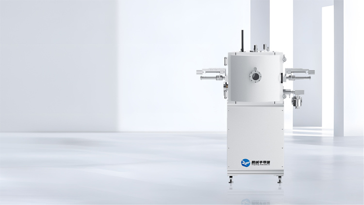
Plasma-Enhanced Chemical Vapor Deposition (PECVD) Equipment : In chemical vapor deposition, excited gases are used to generate low-temperature plasma, enhancing the chemical reactivity of the reactants and enabling epitaxial growth. The primary advantages of plasma-enhanced chemical vapor deposition include low deposition temperatures, minimizing impact on the substrate's structure and physical properties; excellent uniformity in film thickness and composition; dense film structures with few pinholes; strong adhesion between the film and substrate; and a wide range of applications, allowing the preparation of various metal films, inorganic films, and organic films. Pengcheng Semiconductor’s PECVD uniquely features a dual-frequency mode—where the intermediate frequency boosts energy, while the radio frequency increases flux.
Pengcheng Semiconductor is rooted at the intersection of "technological, market, and industrial frontiers," dedicated to equally prioritizing original innovation and tackling key technological challenges. Focusing on industry pain points and domestic production bottlenecks, the company strives to advance the independent control of critical core technologies, paving the way for a secure, reliable, and domestically sourced alternative in high-end equipment. The company specializes in the R&D, design, and full-scale manufacturing of micro- and nano-materials—particularly semiconductor materials—and advanced process technology services and equipment.
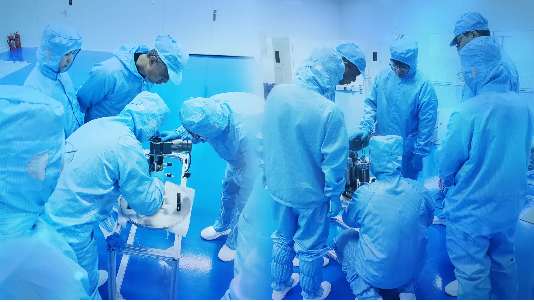
The company boasts a scientifically structured and well-balanced talent team, seamlessly integrating a high-caliber materials and process research group composed of university professors and PhDs with an experienced equipment design team drawn from the industry. Together, they bring over 30 years of accumulated expertise and industry insights in areas such as micro- and nanomaterials and devices, PVD/CVD deposition, epitaxial growth, and comprehensive design and engineering delivery of thin-film equipment systems. Currently, Pengcheng Semiconductor serves a diverse clientele that includes core users in the defense industry, leading defense research institutes, technology-related publicly listed companies, top-tier national key laboratories, and prestigious national-level talent teams—including experts from the "Thousand Talents Program," Yangtze River Scholars, and other overseas high-caliber professionals.
This time at the exhibition, Pengcheng Semiconductor not only showcased its pioneering role as an industry innovation leader but also contributed "Shenzhen Wisdom" to building an open and collaborative global tech ecosystem, helping China's semiconductor industry step onto the international stage with greater competitiveness.
News Center
“The Coating Black Technology” Hidden in Medical Imaging

Contact: Miss Dai
Address: 1704, Building 1, Chongwen Park, Nanshan Zhiyuan, 3370 Liuxian Avenue, Nanshan District, Shenzhen City, Guangdong Province
Shenyang Office Address: Shenyang University Science Park, No.15 Wanghua South Street, Dadong District, Shenyang City, Liaoning Province
Telephone:13632750017
E-mail:sales@hitsemi.com

Message