

Pengcheng Semiconductor Showcases Focus on 'Bottleneck' and 'Cutting-Edge' Fields - 2025 China Materials Conference
Release time:
2025-06-24


“China Materials Congress 2025”: As a national-level academic brand conference in the field of new materials, it is oriented towards major national needs, bringing together the most authoritative experts and scholars and national strategic scientific and technological forces, focusing on key breakthroughs in "stuck neck" areas and "cutting-edge competition" areas, promoting high-end academic discussions, solving major common problems in industry development and major difficulties in the advancement of emerging industries, seizing the academic commanding heights of global new material development, forming a systematic national strategic layout, and building a solid material foundation and guarantee for promoting the construction of China's new productive forces.
“China Materials Congress 2025” will be held at the Xiamen International Convention and Exhibition Center in Fujian Province from July 5th to 8th.
At that time, Pengcheng Semiconductor will showcase its cutting-edge thin film deposition equipment and technical solutions at booth C3094. Based on PVD/CVD technology Magnetron sputtering technology for single-crystal thin film preparation, applying magnetron sputtering to Molecular Beam Epitaxy beam source, etc.
Vacuum coating technology is widely used in electronics, optical instruments, medical devices, new energy, lighting, automobiles, machinery, aerospace and many other fields. For example, in the electronics industry, vacuum coating technology is used to prepare semiconductor devices, microelectronic devices, reflective surfaces, insulating protective coatings, high-temperature sensors, etc. In addition, vacuum coating technology can also improve the physical and chemical properties and service life of the substrate, and has little environmental pollution.
Pengcheng Semiconductor mainly focuses on product improvement, optimization and iteration, improving technical barriers, and deeply exploring user needs to solve industry pain points; in product principle and method classification product coverage PVD Physical Vapor Deposition 、 CVD Chemical Vapor Deposition 、 Molecular Beam Epitaxy thin film growth equipment MBE 。
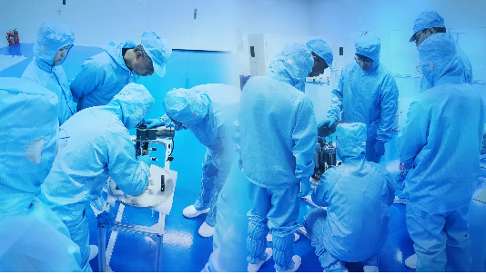
Pengcheng Semiconductor adopts a dual-drive model, with processes and equipment iterating and promoting each other, so that the materials produced by the equipment are optimized to a better level, improving competitiveness. More specifically: (1) Raising magnetron sputtering technology to an ultra-high vacuum level, using PVD technology to epitaxially grow gallium nitride single crystals in a super-clean background. (2) Including but not limited to solving Hot-wire CVD the problem of easy adhesion between hot wires when there are many hot wires, solving the problem of broken wires during long-term use, and developing a large-size polycrystalline diamond wafer growth process.
In short, Pengcheng Semiconductor will showcase its latest breakthroughs in "stuck neck" and "cutting-edge competition" areas at the China Materials Congress 2025. We look forward to exchanging and cooperating with industry colleagues to jointly promote the sustainable development of the semiconductor industry.
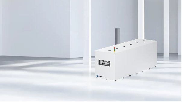
Production-type TGV/TSV/TMV high-vacuum magnetron sputtering coating machine
News Center
Principles, Classification, and Applications of Physical Vapor Deposition (PVD) Technology

Contact: Miss Dai
Address: 1704, Building 1, Chongwen Park, Nanshan Zhiyuan, 3370 Liuxian Avenue, Nanshan District, Shenzhen City, Guangdong Province
Shenyang Office Address: Shenyang University Science Park, No.15 Wanghua South Street, Dadong District, Shenyang City, Liaoning Province
Telephone:13632750017
E-mail:sales@hitsemi.com

Message