

Pengcheng Semiconductor has been awarded the title of National High-tech Enterprise, leading a new journey in nano and atomic manufacturing technology.
Release time:
2025-03-07


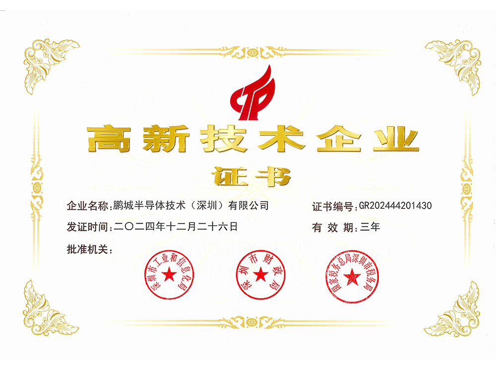
In the current era of rapid technological development, the semiconductor industry, as the cornerstone of modern information technology, is continuously driving innovation and transformation in various fields. Recently,Pengcheng Semiconductor Technology (Shenzhen) Co., Ltd.With its outstanding technological innovation capabilities and significant contributions in the semiconductor field, it has successfully obtained the national high-tech enterprise certification. This honor is not only a high recognition of Pengcheng Semiconductor's past efforts but also marks the authoritative certification of its leading position in the field of nano and atomic manufacturing technology.
Pengcheng Semiconductor was established in 2021, jointly initiated by Harbin Institute of Technology (Shenzhen) and a team of engineers with many years of practical experience. Since its establishment, the company has always been positioned at the intersection of technological and market frontiers, dedicated to solving industry pain points, overcoming localization challenges, and striving for the self-controllability of the industrial chain. Its core business focuses on micro-nano technology and high-end precision manufacturing, covering multiple key areas such as the research and development, design, and production of semiconductor materials, semiconductor processes, and semiconductor equipment.
In terms of technological research and development, Pengcheng Semiconductor has demonstrated strong strength and innovative spirit. The PVD (Physical Vapor Deposition)/CVD (Chemical Vapor Deposition) technology based on nano and atomic manufacturing is one of Pengcheng Semiconductor's core technologies. This technology can achieve high-quality thin film preparation, providing a solid guarantee for the performance improvement of semiconductor devices. For example, the preparation of single crystal thin films through magnetron sputtering technology, and the application of magnetron sputtering in molecular beam epitaxy source, these innovative applications have led to significant achievements for Pengcheng Semiconductor in the field of thin film preparation.

The acquisition of national high-tech enterprise certification has profound significance for Pengcheng Semiconductor. On one hand, it is a high affirmation of the company's technological innovation capabilities and research level, which helps enhance the company's brand image and market competitiveness, attracting more outstanding talents and quality resources, injecting new momentum into the company's sustainable development. On the other hand, the policy support and preferential measures brought by the high-tech enterprise certification will provide strong guarantees for the company's R&D investment and industrial upgrading, further promoting the company's innovation and development in cutting-edge fields such as nano and atomic manufacturing technology.
Looking to the future, Pengcheng Semiconductor will take this opportunity of obtaining national high-tech enterprise certification to continue increasing investment in technological research and development, constantly enhancing its innovation capabilities and core competitiveness. The company will continue to deepen its focus on semiconductor core technology fields such as PVD/CVD technology based on nano and atomic manufacturing, committed to developing more innovative and forward-looking products and solutions, contributing more wisdom and strength to the development of the semiconductor industry. At the same time, Pengcheng Semiconductor will actively strengthen cooperation and communication with domestic and foreign universities, research institutions, and enterprises, jointly promoting technological progress and industrial upgrading in the semiconductor industry, and striving for the self-controllability and high-quality development of China's semiconductor industry.
News Center

Contact: Miss Dai
Address: 1704, Building 1, Chongwen Park, Nanshan Zhiyuan, 3370 Liuxian Avenue, Nanshan District, Shenzhen City, Guangdong Province
Shenyang Office Address: Shenyang University Science Park, No.15 Wanghua South Street, Dadong District, Shenyang City, Liaoning Province
Telephone:13632750017
E-mail:sales@hitsemi.com

Message