

The global MBE market is steadily growing, with China's Pengcheng Semiconductor breaking through technological monopolies
Release time:
2025-05-23


01 Global MBE Market Overview
In 2021, the global Molecular Beam Epitaxy (MBE) system market was approximately 550 million RMB. Looking ahead to 2028, this figure is projected to climb to 960 million RMB, signifying a continuous expansion of the market at a compound annual growth rate (CAGR) of 8.3% between 2022 and 2028. Molecular beam epitaxy systems play a crucial role in semiconductor and basic materials research. The main consumers include countries with well-established industrial systems such as Europe, the United States, Japan, and China, which together account for over 80% of the global market share.

Tracing back Molecular Beam Epitaxy (MBE) technology to its origins, we find it stems from vacuum deposition methods and is based on Arthur's in-depth research in 1968 on the reaction dynamics of gallium arsenide atoms and their interaction with the GaAs surface. This technology was further refined and promoted in the early 1970s by Cho at Bell Labs in the United States, laying a solid foundation for the development of ultrathin layer microstructural materials and related semiconductor science and technology. As a flexible epitaxial thin film technology, molecular beam epitaxy allows the growth of high-quality thin film materials or materials that meet specific structural requirements in an ultra-high vacuum environment by projecting thermally evaporated atomic or molecular beams onto a clean substrate of a specific orientation and temperature.
Looking to the future, the molecular beam epitaxy system market is expected to continue its robust growth. As core equipment for research into new semiconductor and photovoltaic materials and processes, the global molecular beam epitaxy system market reached $81.48 million in 2020 and is projected to reach $111 million by 2026, with a CAGR of 5.26%. This trend indicates the continued prosperity of the molecular beam epitaxy system market globally.
02 China Market and Company Performance
Europe is currently the world's largest producer of molecular beam epitaxy systems with its products widely exported to many countries around the world, while China mainly relies on imports . However, the Chinese national enterprise Pengcheng Semiconductor Technology (Shenzhen) Co., Ltd. (hereinafter referred to as: Pengcheng Semiconductor) has launched a "Molecular Beam Epitaxy (MBE) System" solution, aiming to break this import dependence. Pengcheng Semiconductor's molecular beam epitaxy thin film growth equipment can achieve epitaxial growth processes on specific substrate materials, including the manufacturing of molecular self-assembly, superlattices, quantum wells, and one-dimensional nanowires. In addition, it can also be used for process verification and epitaxial wafer production of second-generation and third-generation semiconductors.
Pengcheng Semiconductor's equipment supports high-quality epitaxial growth of semiconductor materials, is comprehensive in functionality, and is at the international leading level in technology. Its MBE system is not only comprehensive in functionality but also has significant technological advantages. It can successfully achieve epitaxial growth of second-generation semiconductor materials, such as gallium arsenide, and third-generation semiconductor materials, such as silicon carbide and gallium nitride. This groundbreaking achievement further consolidates our technological leadership in the semiconductor field.
03 Equipment Composition and Technical Indicators
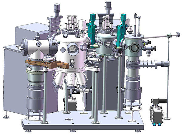
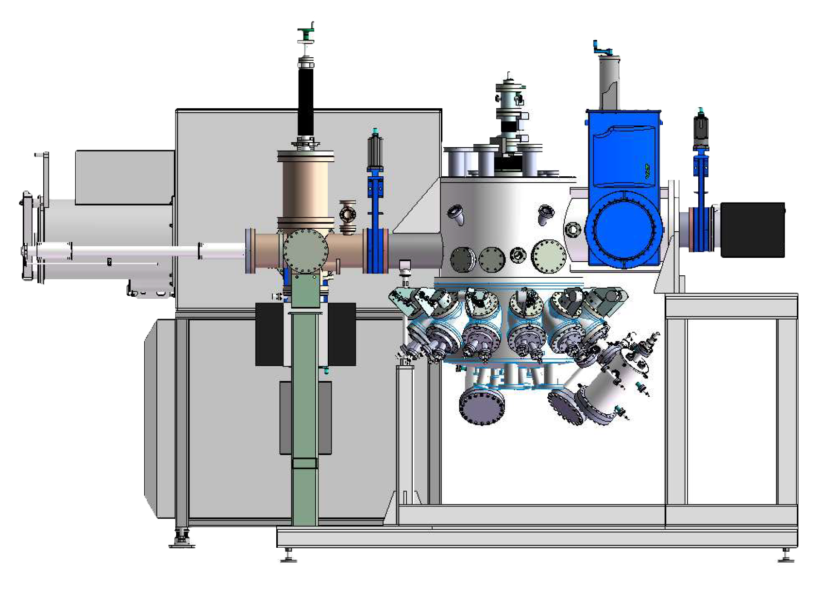
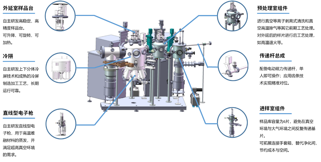
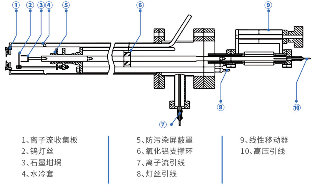
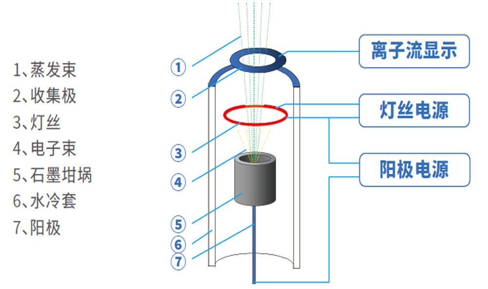
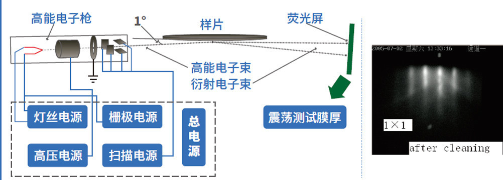
MBE equipment includes multiple chambers and key components, all independently researched and designed for high performance. In 2005, this project was the first in China to complete the research, development, design, and manufacturing of a complete set of domestically produced MBE, achieving independent control. Pengcheng Semiconductor independently designed core components such as the MBE ultra-high vacuum epitaxial growth chamber, process control system and software, in-situ real-time RHEED monitoring instrument, linear electron gun, high-temperature effusion cell, effusion cell power supply, high-temperature sample stage, and film thickness meter. These innovative designs have enabled Pengcheng Semiconductor's MBE system to achieve internationally leading levels in performance and precision, effectively breaking the monopoly of foreign products.
Equipment Composition:
- Loading Chamber : Used for sample loading and unloading, equipped with multi-wafer storage function, accommodating six substrates.
- Pre-treatment Chamber : Used for vacuum plasma stripping cleaning, vacuum high-temperature degassing, and other pre-process treatments before samples enter the epitaxial chamber.
- Epitaxial Chamber : An ultra-high vacuum clean vacuum chamber specifically for molecular beam epitaxy processes.
The ultimate vacuum and temperature control of each chamber reaches internationally advanced levels, with flexible configuration suitable for diverse processes. Its main technical indicators include:
- Loading Chamber: Ultimate vacuum reaches 5.0 × 10^-5 Pa, can load 6 samples with sizes ranging from φ2 inches to φ4 inches.
- Pre-treatment Chamber: Ultimate vacuum is 5 × 10^-7 Pa, sample stage heating temperature range from room temperature to 850℃ ± 1℃.
- Epitaxial Chamber: Ultimate vacuum reaches 2.0 × 10^-8 Pa, sample stage heating temperature range from room temperature to 1200℃ ± 1℃.
04 Products and Application Examples
Component design meets high vacuum and high temperature requirements, combined with advanced technology, to support precise epitaxial production. This MBE system is not only comprehensive in functionality but also has significant technological advantages. It can successfully achieve epitaxial growth of various semiconductor materials.
Pengcheng Semiconductor's equipment It has been successfully used to produce specific new materials, demonstrating technological potential and will continue to drive technological innovation. The equipment uses Pengcheng Semiconductor's self-developed molecular beam epitaxy equipment to successfully grow Bi2-xSbxTe3 material. Pengcheng Semiconductor continues to cultivate the molecular beam epitaxy technology field, continuously breaking through core difficulties.
Looking to the future, Pengcheng Semiconductor will closely monitor market trends, actively cultivate a deep understanding of end-user applications and customer needs to enhance close ties with customers. Pengcheng Semiconductor's goal is to provide customers with unique value-added services to support their business development. At the same time, Pengcheng Semiconductor will continue to innovate with a grateful heart, striving to achieve new and greater achievements at the forefront of semiconductor epitaxial technology.
News Center
Application of TGV Glass Through-Hole Technology in Magnetron Sputtering
Pengcheng Semiconductor: The Strategy, Tactics, and Survival Guide of a High-Tech Enterprise

Contact: Miss Dai
Address: 1704, Building 1, Chongwen Park, Nanshan Zhiyuan, 3370 Liuxian Avenue, Nanshan District, Shenzhen City, Guangdong Province
Shenyang Office Address: Shenyang University Science Park, No.15 Wanghua South Street, Dadong District, Shenyang City, Liaoning Province
Telephone:13632750017
E-mail:sales@hitsemi.com

Message