

Pengcheng Semiconductor Hard Coating and Film Deposition Solutions: Empowering High-End Manufacturing Performance
Release time:
2025-08-05


In the arena of high-end manufacturing, every technological breakthrough is like a shining new star, illuminating the path forward for the industry. Pengcheng Semiconductor Technology (Shenzhen) Co., Ltd. (hereinafter referred to as: Pengcheng Semiconductor ), as an innovation pioneer in the industry, with its excellent hard coating and film deposition solutions, is injecting strong impetus into the improvement of high-end manufacturing performance, becoming a trusted partner for many enterprises.
Pengcheng Semiconductor was jointly established by Harbin Institute of Technology (Shenzhen) and a team of engineers with many years of practical experience. The company is rooted at the intersection of industry, technology, and market frontiers, with a mission to solve industry pain points and achieve independent and controllable industrial chains. It has been deeply involved in micro-nano technology and high-end precision manufacturing, especially showing extraordinary strength in hard coating and film deposition technology.
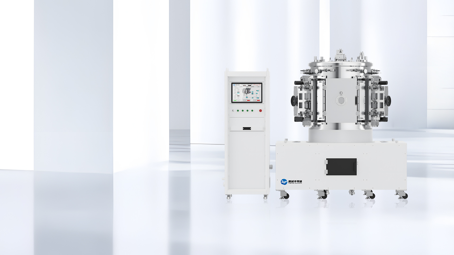
Advanced Film Deposition Technology System
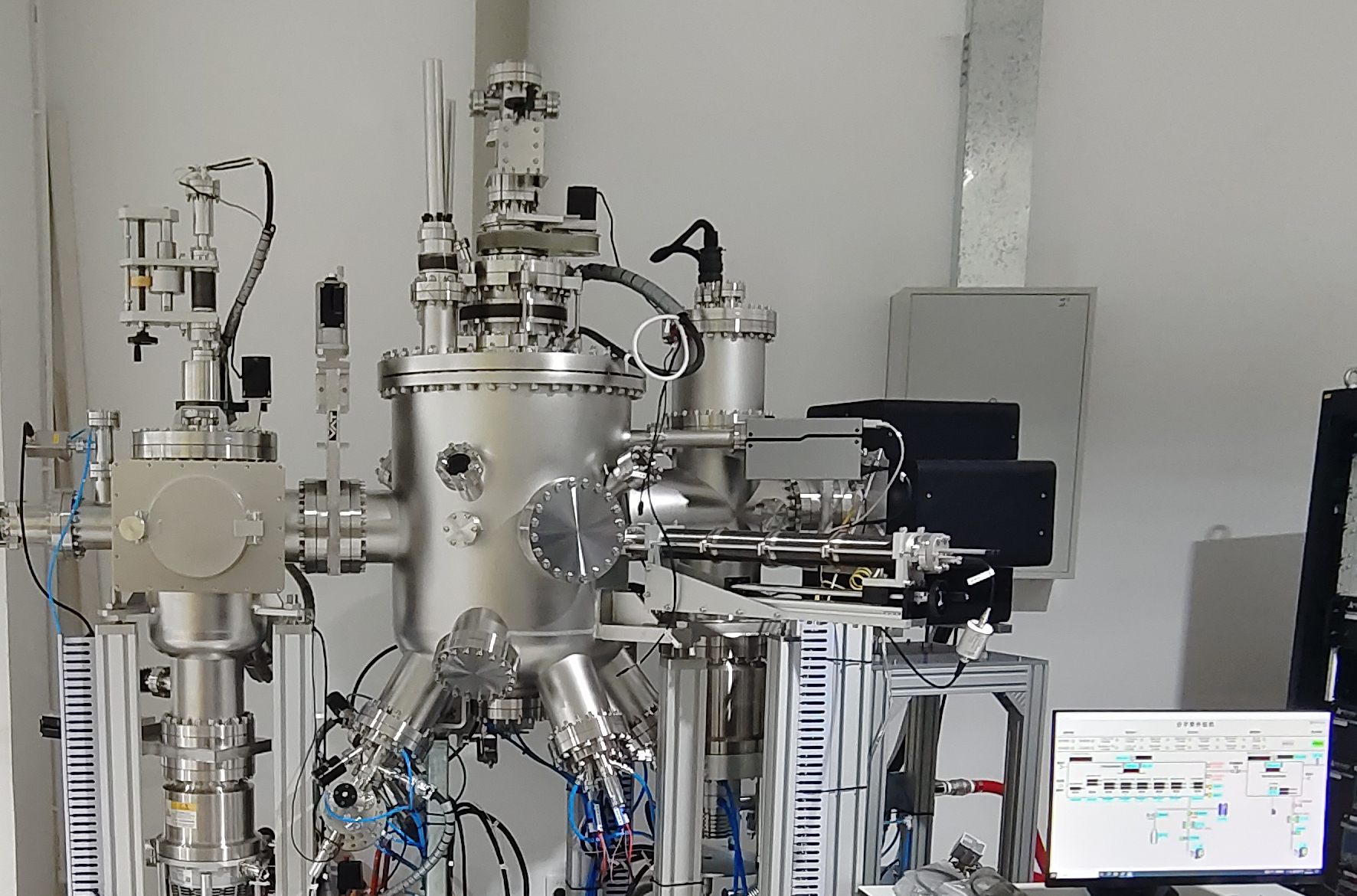
Pengcheng Semiconductor possesses a complete and advanced hard coating and film deposition technology system, covering a variety of cutting-edge processes. Its Hot Filament Chemical Vapor Deposition (HFCVD) solution is a powerful tool for the production of microcrystalline and nanocrystalline diamond wafers. Through this technology, hard coatings with excellent corrosion resistance and wear resistance can be manufactured, exhibiting excellent performance in the heat sink applications of high-power devices, high-frequency devices, and high-power lasers. Furthermore, this technology can also be used in the production of corrosion-resistant diamond conductive electrodes for wastewater treatment in the environmental protection field, demonstrating broad application prospects.
Hot Filament Chemical Vapor Deposition (HFCVD)
In the field of high-vacuum PVD film deposition technology, Pengcheng Semiconductor also has profound expertise. This technology utilizes evaporation or sputtering under vacuum conditions to deposit various thin films on the substrate surface, ranging from metals and alloys to compounds, semiconductors, and ceramics. Whether it is single-layer films, multi-layer films, doped films, or alloy films, they can be precisely deposited, and can even be used for the deposition of magnetic and non-magnetic materials. It is particularly noteworthy that Pengcheng Semiconductor has upgraded magnetron sputtering thin film deposition technology to thin film epitaxy technology , this domestically pioneering breakthrough has been applied to the epitaxial process of third-generation semiconductor GaN and fourth-generation semiconductor Ga2O3.
Diverse Equipment Support
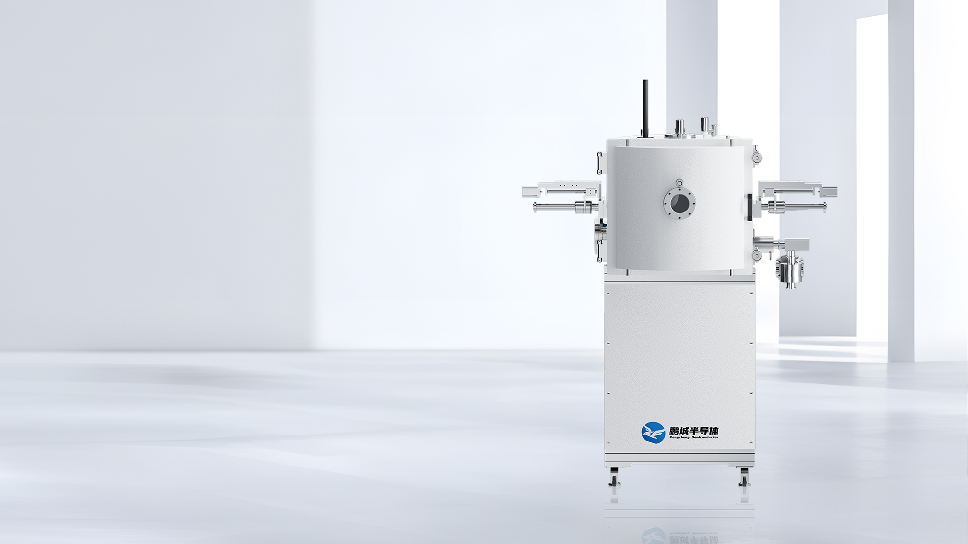
To ensure hard coating and film deposition solution implementation efficiency, Pengcheng Semiconductor is equipped with a series of advanced equipment. Production-type TGV/TSV/TMV high-vacuum magnetron sputtering coating machine , in the high-density through-holes and blind hole coating of glass and ceramic substrates, shows significant advantages, with an aspect ratio of up to 10:1 . In the substrate coating process, it excels in the deposition of Cu/Ti microstructures and Au/TiW transmission line dual-system films, providing strong support for improving the integration density of microsystems. This equipment features high film uniformity and repeatability, strong adhesion, and programmable automated control based on process recipes, greatly improving production efficiency and product quality.
Production-type TGV/TSV/TMV high-vacuum magnetron sputtering coating machine
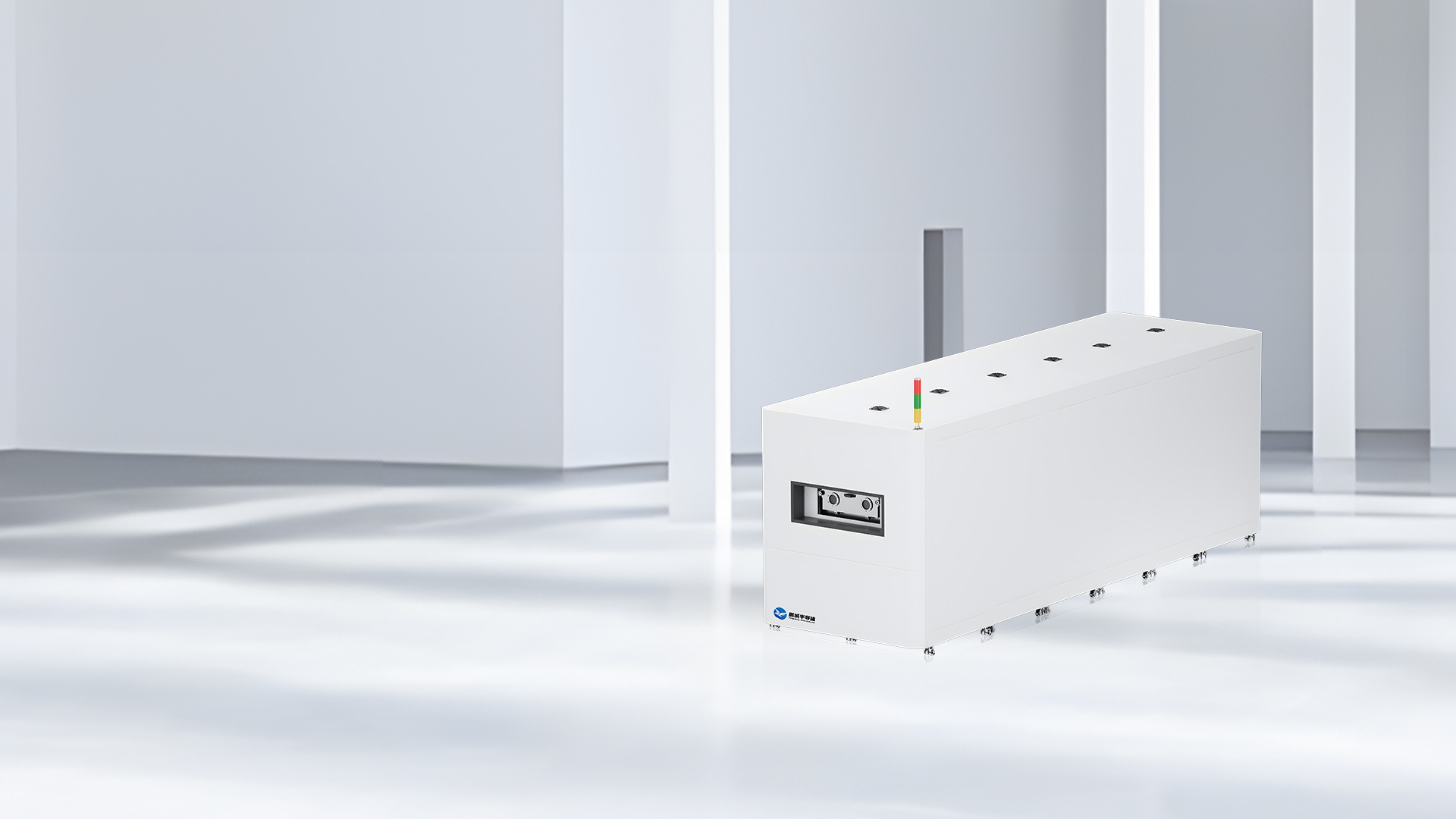
Production-type high-vacuum magnetron sputtering and ion-assisted composite coating machine has a wide range of applications. From milling cutters and drills to bearings, gears, and lenses, hard and wear-resistant coatings can be prepared on their surfaces using this equipment. It integrates various process methods such as workpiece surface treatment, ion cleaning, particle control, magnetron sputtering, ion-assisted coating, and reactive sputtering coating, and can prepare a wide variety of films such as single-layer films, multi-layer films, doped films, metal films and alloy films, and compound thin films to meet the complex needs of various high-end manufacturing fields.
Production-type high-vacuum magnetron sputtering and ion-assisted composite coating machine
Significant Application Effectiveness
Pengcheng Semiconductor's hard coating and film deposition solutions have achieved remarkable results in practical applications. In the semiconductor manufacturing field, its advanced coating technology provides high-quality thin films for chip manufacturing. The uniform and stable film quality greatly improves chip performance, helping the semiconductor industry move towards higher processes and lower power consumption. In advanced packaging, the technological breakthroughs of the high-vacuum magnetron sputtering coating machine have made the application of glass and ceramic substrates in 3D packaging and heterogeneous integration more extensive, accelerating the miniaturization and high-performance development trend of chips, and providing key technological support for the thinning and high-performance of electronic products.
In the machinery manufacturing industry, Pengcheng Semiconductor's hard and wear-resistant coatings significantly improve the service life of tools, bearings, gears, lenses, etc. Taking milling cutters as an example, after hard coating and film deposition treatment, the wear resistance of the tools is greatly improved, and they can maintain sharpness for a longer time during cutting, reducing the frequency of tool changes, improving processing efficiency, and reducing production costs. At the same time, the good adhesion of the coating ensures that the coating is not easily detached under complex working conditions, ensuring the stability of processing and product quality.
Professional Team Guarantee
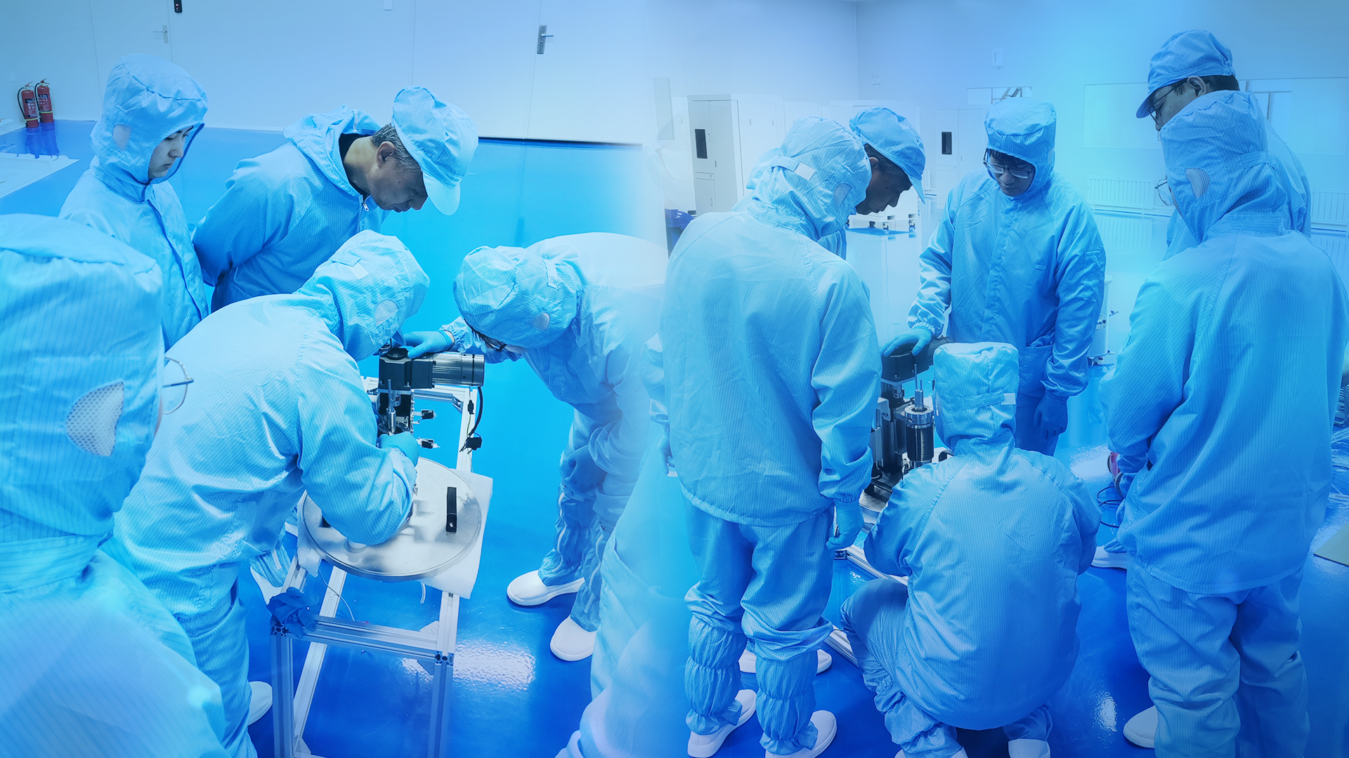
The success of Pengcheng Semiconductor is inseparable from its professional talent team. The company has a high-level materials research and process research team centered on professors and doctors from Harbin Institute of Technology. They, with their profound academic achievements and cutting-edge scientific research concepts, continuously explore new directions in hard coating and film deposition technology. In addition, the senior equipment design team from the industry has over 30 years of experience in semiconductor material research, epitaxial technology research, and the design, production, and manufacturing of complete sets of semiconductor thin film preparation equipment, combining rich practical experience with advanced technological concepts to provide a solid guarantee for the company's product research and development and solution formulation.
Pengcheng Semiconductor Technology (Shenzhen) Co., Ltd.'s hard coating and film deposition solutions provide comprehensive support for enhancing high-end manufacturing performance, leveraging its advanced technological system, diverse equipment support, remarkable application results, and professional team. In the future, with continuous technological innovation and expansion of application fields, Pengcheng Semiconductor will play an even more important role in the high-end manufacturing sector, joining hands with more enterprises to usher in a new chapter of high-end manufacturing.
News Center
Principles, Classification, and Applications of Physical Vapor Deposition (PVD) Technology

Contact: Miss Dai
Address: 1704, Building 1, Chongwen Park, Nanshan Zhiyuan, 3370 Liuxian Avenue, Nanshan District, Shenzhen City, Guangdong Province
Shenyang Office Address: Shenyang University Science Park, No.15 Wanghua South Street, Dadong District, Shenyang City, Liaoning Province
Telephone:13632750017
E-mail:sales@hitsemi.com

Message