 Co.,Ltd.")

Semiconductor manufacturing and advanced packaging continue to heat up
Release time:
2025-02-27


Thanks to strong policy support, cyclical changes in the industry, innovation-driven growth, and the accelerated promotion of domestic substitution, the localization rate has significantly improved across multiple segments from IC design to wafer manufacturing, packaging testing, and equipment materials, marking a steady progress of China's semiconductor industry towards self-control.
The localization rate of semiconductor materials is still further improving.
By 2025, the annual growth rate of global semiconductor capacity will reach 6.6%, with 33.6 million wafers produced each month, while mainstream process capacity will achieve a 6% growth, reaching 15 million wafers per month. Compared to advanced processes, mature process nodes have lower technology requirements for semiconductor materials, providing a rare opportunity for domestic semiconductor material manufacturers to push their products into the supply chain.
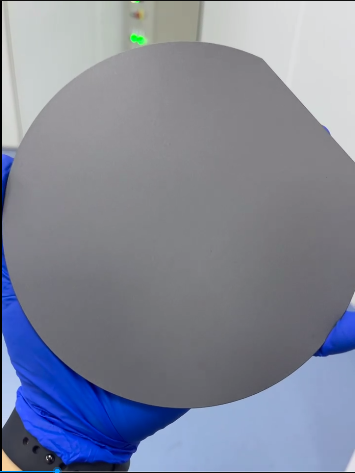
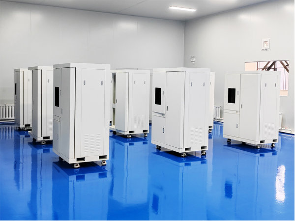
HFCVD diamond film deposition equipment
China's high demand will continue to drive equipment sales growth.
Since the 13th Five-Year Plan, policies such as "Made in China 2025," the 14th Five-Year Plan, and the National Integrated Circuit Industry Investment Fund (referred to as the "Big Fund") have continuously strengthened support, injecting strong momentum into the semiconductor equipment industry and building a comprehensive and multi-dimensional policy support system. By 2025, the equipment market will see strong growth, with an expected increase of 19.6%, primarily driven by China's sustained high demand. Currently, the development of industries such as artificial intelligence (AI), big data, and storage chips is pushing the global semiconductor industry towards a trillion-dollar market scale, which will undoubtedly provide more market opportunities and development space for semiconductor equipment manufacturers.
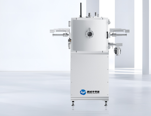
Production-type high vacuum magnetron sputtering/ion-assisted/multi-arc composite coating machine
The importance of advanced packaging in manufacturing processes is becoming increasingly prominent.
By 2025, advanced packaging will continue to be a more important component of semiconductor manufacturing processes, helping to optimize power, performance, and area while reducing costs. AI is driving the demand for larger substrates with more layers and I/O. To continue Moore's Law and keep pace with innovations in the high-end computing market, advanced packaging has become a core strategy to meet the demands of these high-performance applications.

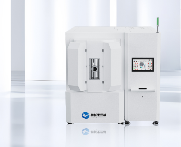
Production-type TGV/TSV/TMV high vacuum magnetron sputtering coating machine
Driven by the dual forces of technological innovation and market demand, Pengcheng Semiconductor presents cutting-edge technologies, core products, and solutions in the fields of semiconductor materials, semiconductor equipment, and advanced packaging.

Production-type high vacuum magnetron sputtering and ion-assisted composite coating machine
Company Introduction:
Pengcheng Semiconductor Technology (Shenzhen) Co., Ltd. was jointly initiated by Harbin Institute of Technology (Shenzhen) and a team of engineers with many years of practical experience. The company is based at the intersection of technological and market frontiers, seeking innovation leadership and sustainable development, addressing industry pain points and localization challenges, and striving for self-control in the industrial chain.
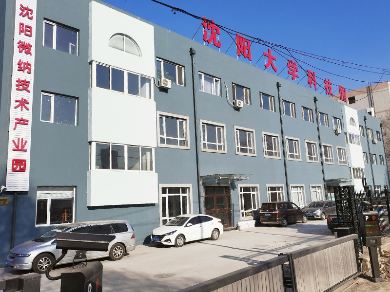
Pengcheng Micro-Nano Technology (Shenyang) Co., Ltd. is a wholly-owned subsidiary of Pengcheng Semiconductor Technology (Shenzhen) Co., Ltd., serving as the design center and production base for semiconductor processes and equipment.
The company's core business is micro-nano technology and high-end precision manufacturing, with specific application areas including research and design, production, process technology services, and upgrading of semiconductor materials, processes, and equipment, providing users with process research and sample testing.
The company's talent team has a complete knowledge structure, with a high-level materials research and process research team centered around professors and doctors from Harbin Institute of Technology; there is also a team of senior equipment designers from the industry, who have over 20 years of experience in semiconductor materials research, epitaxial technology research, and the design and production of complete equipment for semiconductor thin film preparation.
The company relies on Harbin Institute of Technology (Shenzhen) and possesses advanced semiconductor R&D equipment platforms and testing equipment platforms, enabling high-level scientific research work. The company is headquartered in Shenzhen and has the capabilities for R&D, production, debugging of semiconductor equipment, as well as pilot production, manufacturing, and sales of semiconductor materials and devices.
News Center
TSV Technology: A Core Pillar of AI Computing Power

Contact: Miss Dai
Address: 1704, Building 1, Chongwen Park, Nanshan Zhiyuan, 3370 Liuxian Avenue, Nanshan District, Shenzhen City, Guangdong Province
Shenyang Office Address: Shenyang University Science Park, No.15 Wanghua South Street, Dadong District, Shenyang City, Liaoning Province
Telephone:13632750017
E-mail:sales@hitsemi.com

Message