

Pengcheng Semiconductor showcases TGV/TSV/TMV technology at the Munich Shanghai Optical Expo.
Release time:
2025-02-21


Munich Shanghai Optical Expo, known as the annual event for the laser, optics, and optoelectronics industry in Asia. Since its first session in Shanghai in 2006, its scale and influence have been increasing day by day, and it has become an important communication platform for the global optoelectronics industry.
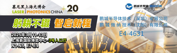
The Munich Shanghai Optical Expo will be held from March 20-22, 2025, at the Shanghai New International Expo Center (No. 2345 Longyang Road, Pudong New District, Shanghai), at which timePengcheng Semiconductorwill showcase cutting-edgethin film deposition equipmentand technical solutions at booth E4-4631. Based on nano and atomic manufacturing,PVD/CVDthe technology is used for high-quality thin film preparation. For example, using magnetron sputtering technology for single crystal thin film preparation, and applying magnetron sputtering to molecular beam epitaxy's beam source, etc. The exhibits cover popular application areas such as micro-nano optics, acoustics, and medical fields. This Munich Shanghai Optical Expo will bring cutting-edge technologies and products to everyone, and we sincerely invite all new and old customers to visit our booth for discussions and exchanges!
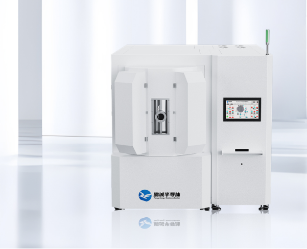
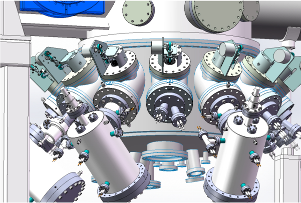
Production-type TGV/TSV/TMV high vacuum magnetron sputtering coating machine
The star product of Pengcheng Semiconductor at this exhibition - production-typeTGV/TSV/TMVhigh vacuum magnetron sputtering coating machine.
This equipment is used forglass substratesandceramic substratesfor high-density through holes and blind holes coating,with a depth-to-diameter ratio >10:1.For example: for substrate coating processes, Cu/Ti microstructures, and Au/TiW transmission line dual system film layer deposition capabilities, providing support for the increase in micro-system integration density.
In terms of coating on glass substrates and ceramic substrates, this coating machine has obvious advantages. Glass substrates, as the next generation of chip substrates, have excellent high-frequency electrical properties, large size, ultra-thin and easy to obtain, low cost, simple process flow, and strong mechanical stability.
Pengcheng Semiconductor's production-type TGV/TSV/TMV high vacuum magnetron sputtering coating machine has achieved multiple innovations and breakthroughs technically, injecting new vitality into the development of the semiconductor industry.

From the perspective of industry development,TGV/TSV/TMVtechnological innovation has driven the progress of the semiconductor industry inadvanced packaging, high-performance chip manufacturing and other key areas. In advanced packaging, the technological breakthroughs of high vacuum magnetron sputtering coating machines have made the application of glass substrates and ceramic substrates more widespread in 3D packaging and heterogeneous integration, accelerating the trend of chip miniaturization and high performance; in high-performance chip manufacturing, uniform and high-quality coating processes ensure the performance improvement of chips, helping to promote the semiconductor industry towards higher processes and lower power consumption.
Production-type high vacuum magnetron sputtering/ion-assisted/multi-arc composite coating machine
This equipment is widely used for the preparation of hard wear-resistant coatings on the surfaces of milling cutters, drill bits, bearings, gears, lenses, etc., integrating workpiece surface treatment, ion cleaning, particulate control, magnetron sputtering, ion-assisted coating, and reactive sputtering coating processes into one PVD equipment.
It can prepare single-layer films, multi-layer films, doped films, metal films, alloy films, compound films, etc.
Production-type high vacuum magnetron sputtering and ion-assisted composite coating machine
Uses magnetron sputtering, ion-assisted, and reactive sputtering processes to prepare various thin film materials on the workpiece surface. This equipment integrates workpiece surface treatment, ion cleaning, particulate control, magnetron sputtering, ion-assisted coating, and reactive sputtering coating processes into one PVD equipment.
It can prepare single-layer films, multi-layer films, doped films, metal films, alloy films, compound films, etc.

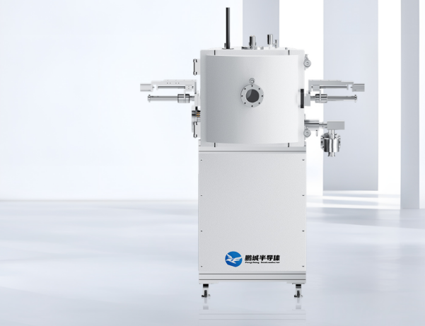
Research-type high vacuum magnetron sputtering coating machine
The research-type high vacuum magnetron sputtering machine Circular Sputter series is our company's research-type high vacuum magnetron sputtering instrument, mainly using circular magnetron sputtering targets for sputtering methods to prepare metals, alloys, compounds, semiconductors, ceramics, dielectric composite films, and other chemical reaction films; suitable for coating various single-layer films, multi-layer films, doped films, and alloy films; can coat magnetic and non-magnetic materials.
Can be used for the research and development of TGV/TSV/TMV advanced packaging, deep hole seed layer coating with a high depth-to-diameter ratio (≥10:1).
Key technical features of the equipment
Adhering to the concept that equipment provides means for process realization, we have made the following designs and engineering implementations, with good actual operation effects, providing precise process equipment solutions for users' specialized process realization.
HFCVD hot wire chemical vapor deposition equipment
Developed and designed hot wire CVD diamond equipment, divided into experimental equipment and production equipment.
The equipment is mainly used for the research and production of microcrystalline and nanocrystalline diamond films. It can be used for the research and production of diamond products at mechanical, thermal, optical, and acoustic levels.
Can manufacturelarge-size diamondspolycrystalline wafers, used for heat sinks of high-power devices, high-frequency devices, and high-power lasers.
Can be used to produce anti-corrosion and wear-resistant hard coatings; diamond products for wastewater treatment in the environmental field.
Can be used for diamond film preparation on flat workpieces, and can also be used for diamond hard coating preparation on tool surfaces or other irregular surfaces.
Can be used for the research and production of solar thin film batteries.
MBE molecular beam epitaxy equipment
Molecular Beam Epitaxy (MBE) equipment can achieve epitaxial growth processes on certain substrates, enabling molecular self-assembly, superlattices, quantum wells, one-dimensional nanowires, etc. It can be used for process verification and epitaxial wafer growth and manufacturing of second-generation and third-generation semiconductors.

The molecular beam epitaxy thin film growth experimental equipment designed and manufactured by our company comes in two types: experimental and production. It has a reasonable configuration, simple structure, convenient operation, advanced technology, reliable performance, multiple applications, strong practicality, and a relatively low Price, making it suitable for laboratories and research institutions in universities for teaching experiments, scientific research, and process experiments in the field of molecular beam epitaxy.
Production-type MBE can be used for the preparation of small batches of epitaxial wafers.
News Center

Contact: Miss Dai
Address: 1704, Building 1, Chongwen Park, Nanshan Zhiyuan, 3370 Liuxian Avenue, Nanshan District, Shenzhen City, Guangdong Province
Shenyang Office Address: Shenyang University Science Park, No.15 Wanghua South Street, Dadong District, Shenyang City, Liaoning Province
Telephone:13632750017
E-mail:sales@hitsemi.com

Message