 Co.,Ltd.")

Principle of Vacuum Coating Machine Equipment
Release time:
2024-11-28


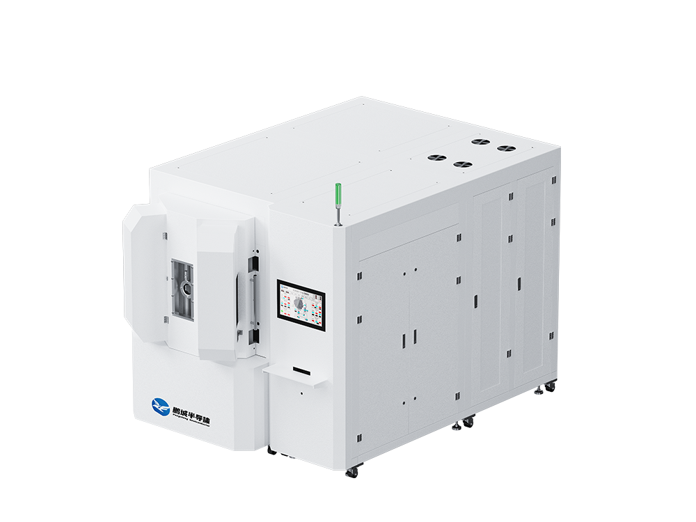
Vacuum Coating Machineis an advanced surface treatment technology device that can form one or more layers of thin films on the surface of various materials, giving the substrate new properties such as improved wear resistance, corrosion resistance, and optical performance. The working principle of the vacuum coating machine is mainly based on physical vapor deposition (PVD) technology, involving various physical processes such as vacuum technology, thermal evaporation, and sputtering.
In these processes, the working principle of the vacuum coating machine can be summarized in the following key steps:
1. Creation of a vacuum environment: The film material (such as metals, alloys, compounds, etc.) is released by heating and evaporating or sputtering, then freely flies in the vacuum chamber and finally deposits on the substrate surface. This step is crucial because air molecules can collide with the evaporated film molecules, leading to rough and dull crystallinity. A high vacuum environment can significantly reduce such collisions, making the crystallinity dense and bright.
2. Release of film material: In a vacuum environment, the film material is released by heating and evaporating or sputtering.
Evaporation process: Heating the evaporation source causes the film material to evaporate into gaseous molecules. Sputtering process: High-energy particles (such as ions) bombard the target material, causing target atoms or molecules to be ejected.
3. Deposition of molecules: The evaporated or sputtered film molecules freely fly in the vacuum chamber and finally deposit on the substrate surface. During the deposition process, the molecules undergo stages of adsorption, diffusion, and condensation, ultimately forming one or more layers of thin film.
4. Cooling after coating completion: After the coating is completed, the vacuum coating machine needs to be cooled to solidify the film on the substrate. This process helps enhance the bonding strength between the film and the substrate, improving the stability and durability of the film.
Magnetron sputtering technology can significantly improve sputtering efficiency and film quality. It uses a magnetic field to control the motion trajectory of the sputtered target atoms or molecules, allowing for more uniform deposition on the substrate surface.
There are various types of vacuum coating machines, such asevaporation coating machines,sputtering coating machines, ion coating machines, etc., each type has its unique characteristics and applicable scope. For example, evaporation coating machines are suitable for coating metal films and alloy films; sputtering coating machines are suitable for coating high hardness and high wear resistance films; ion coating machines can form films with special properties on the substrate surface.
Vacuum coating technology has wide application value in industrial production. It can provide high-quality surface treatment technology for various industrial products, improving their wear resistance, corrosion resistance, optical performance, etc. At the same time, vacuum coating technology can also provide high-quality protective films and reflective films for optical devices, electronic devices, etc., thereby extending the service life of products and enhancing their performance.
In summary, the working principle of the vacuum coating machine involves multiple complex physical processes and technical links. By precisely controlling these processes, high-quality and high-efficiency coating production can be achieved, providing advanced surface treatment technology for various industrial applications.
Equipment Manufacturer-Pengcheng Semiconductor Technology (Shenzhen) Co., Ltd.
News Center
TSV Technology: A Core Pillar of AI Computing Power

Contact: Miss Dai
Address: 1704, Building 1, Chongwen Park, Nanshan Zhiyuan, 3370 Liuxian Avenue, Nanshan District, Shenzhen City, Guangdong Province
Shenyang Office Address: Shenyang University Science Park, No.15 Wanghua South Street, Dadong District, Shenyang City, Liaoning Province
Telephone:13632750017
E-mail:sales@hitsemi.com

Message