 Co.,Ltd.")

Thin film deposition equipment
Release time:
2025-04-30


One of the three core pieces of equipment in semiconductor production lines is thin film deposition equipment.
I. What is thin film deposition?
Q&A
II. PVD 、 CVD and ALD Detailed introduction
III. Two important industrial PECVD Introduction
What is thin film deposition equipment?
IV. Global Semiconductor Thin Film Deposition Equipment Market
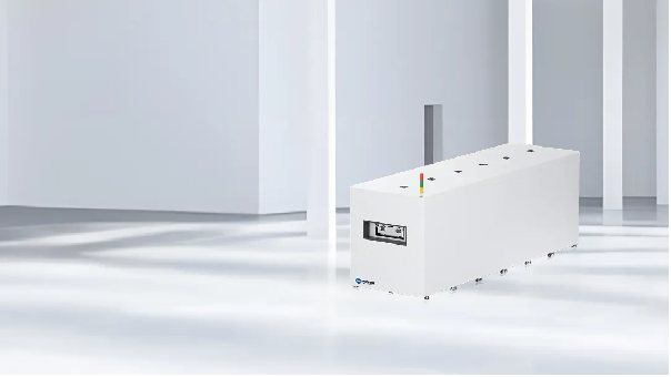
Production-type TGV/TSV/TMV high-vacuum magnetron sputtering coating machine
I. What is thin film deposition?
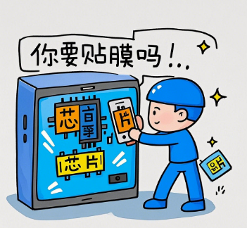
Simply put: Thin film deposition is like applying a 'film' to a chip. 的。
The more precise and layered the chip, the greater the demand for 'film application'.
Better chips require more application.
Professionally speaking: Thin film deposition refers to the deposition of thin film materials to be processed on substrates such as silicon wafers. The deposited thin film materials are mainly non-metals such as silicon dioxide, silicon nitride, and polysilicon, as well as metals such as copper. The deposited film can be amorphous, polycrystalline, or single crystal.

Including CVD (Chemical Vapor Deposition), PVD (Physical Vapor Deposition), and ALD (Atomic Layer Deposition), among which ALD belongs to CVD 's branch.
Q&A:
Why do we say that the more precise and layered the chip, " film application ” " demand increases?
Chip manufacturing is like applying a film to a phone, except this "film" is at the nanometer level and needs to be applied dozens or even hundreds of layers !As chip processes become more precise and structures become more complex, the demand for "film application" increases significantly.
The more advanced the process, the more layers of film
in 90nm process CMOS production lines, approximately 40 thin film deposition processes are required, involving 6 types of materials; while in 3nm process FinFET production lines, the number of thin film deposition processes increases to 100 processes, and the number of materials approaches 20 types. Each layer of "film" is crucial; without any layer, the chip may not function properly.
The more complex the structure, the more difficult it is to apply the film
Taking storage chips as an example, from 2D NAND to 3D NAND ,the structure changes from planar to three-dimensional, and the number of layers increases significantly, like changing from a single-story house to a skyscraper. Each layer requires precise "film application," which naturally leads to rapid growth in the demand for thin film deposition equipment.
Therefore, thin film deposition equipment is the "film application master" in chip manufacturing, and the more precise and layered the chip, the more indispensable it is.
II. PVD, CVD
- PVD Physical Vapor Deposition
Physical vapor deposition is a thin film deposition technology that uses a physical mechanism; the process does not involve chemical reactions.
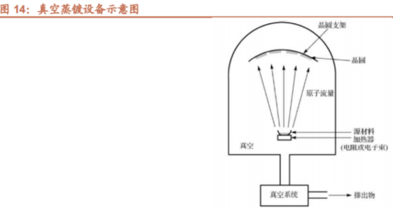
Mainly includes Evaporation 、 Sputtering Arc plasma coating, ion plating, Molecular beam epitaxy etc. Evaporation: Refers to a coating technology in which, in a high-vacuum chamber, the evaporation source of the evaporation material is heated by resistance, electron beam, high-frequency induction, arc, and laser, etc., to reach the melting and vaporization temperature, so that atoms or molecules of the evaporation material are vaporized from its surface to form a vapor stream that is incident on the surface of the substrate to be evaporated and condenses to form a solid thin film.
Vacuum evaporation is the mainstream process for OLED panels.
Sputtering: Usually refers to magnetron sputtering, which utilizes the characteristics of charged particles accelerating in an electric field to have a certain kinetic energy, and in a vacuum state of 1.3 × 10 -3 Pa, inert gas is filled, and a high-voltage DC electric field is applied between the substrate (anode) and the metal target (cathode). Due to the glow discharge, electrons excite inert gases to generate plasma, knocking out atoms from the metal target and depositing them on the substrate.
Sputter coating is the most widely used PVD.
Molecular beam epitaxy (MBE) : This is a special vacuum deposition process, where thin films are grown layer by layer along the crystallographic axis of the substrate material. MBE It can produce single-crystal thin films with tens of atomic layers, as well as films with alternating components and doping to form ultrathin layer quantum microstructures.

Ion plating: A combination of vacuum evaporation and sputtering deposition. After the material to be plated is vaporized, it is partially ionized in the discharge space, and then the ions to be plated are attracted by the electrode to the substrate and deposited into a film.
Due to its complexity, ion plating has a limited range of applications.
In summary, during the PVD process, only the material form changes, and no chemical reaction is involved; it is a purely physical change. In the entire semiconductor manufacturing process, PVD is an indispensable key process for depositing ultra-pure metal and transition metal nitride thin films.
2. CVD Chemical Vapor Deposition
Deposition of dielectric and semiconductor films CVD This is a film deposition process that deposits solid thin films on the surface of a substrate through gas-phase chemical reactions; it is a chemical reaction.
CVD The reaction precursors are generally gaseous raw materials such as silane, phosphine, borane, ammonia, and oxygen. The products are generally solid films such as nitrides, oxides, nitroxides, carbides, and polysilicon. The reaction conditions are generally high temperature, high pressure, plasma, etc.
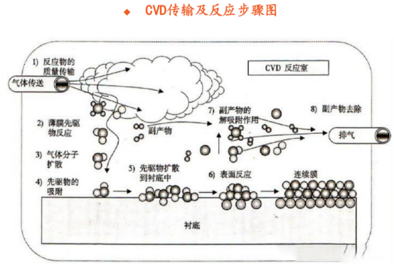
The CVD film formation process generally includes eight steps:
- Reaction gas is transported to the deposition area;
- Film precursor formation;
- Film precursor diffusion to the substrate surface;
- Film precursor adhesion;
- Film precursor diffusion to the film growth area;
- Surface chemical reaction, film precipitation and gradual growth, eventually forming a continuous film, while by-products are generated;
- By-products are removed from the substrate surface;
- By-products are removed from the reaction chamber. With the continuous advancement of the process, the needs for trench and deep hole filling have given rise to new CVD technologies. Currently, the mainstream technologies used are LPCVD 、 PECVD ,and future development directions include HDPCVD 、 SACVD 。
Two important industrial PECVD Introductions:
According to the frequency of plasma generation, PE CVD The plasma used in can be divided into radio frequency plasma ( Radio Frequency Plasma ) and microwave plasma ( Microwave Plasma ) two types.
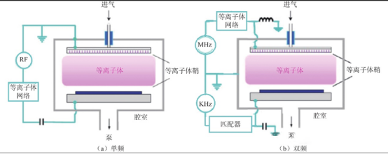
Currently, the radio frequency used in the industry is generally 13.56MHz 。Among them, the radio frequency plasma coupling method is usually divided into Capacitive coupling ( CCP ) and Inductive coupling ( ICP ) ) two types.
3. ALD Atomic Layer Deposition
ALD It has the ability to precisely control film thickness, the thickness uniformity and consistency of the deposited film is extremely excellent, and its step coverage capability is very strong, suitable for film growth in deep trench structures. ALD in SADP 、 HKMG ,plays an important role in many processes such as metal copper interconnect diffusion barrier layers.
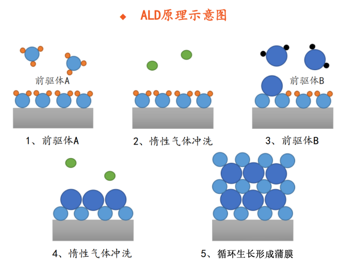
ALD Principle : By alternately introducing gas-phase precursors into the reactor and forming films in a monolayer manner on the substrate surface, the reaction steps include:
1 ) precursor A enters the reaction chamber and adsorbs on the substrate surface;
2 ) Inert gas flushes the reaction chamber, removing the remaining precursor A clean;
3 ) precursor B enters the reaction chamber and adsorbs on the substrate surface, reacting with the precursor A to generate the target thin film;
4 ) Inert gas flushes the reaction chamber, removing the by-products generated by the chemical reaction from the reaction chamber, completing one atomic layer thin film deposition. By repeating this cycle, thin film deposition at the unit atomic layer level can be achieved.
Three. What is thin film deposition equipment
Thin film deposition is a key semiconductor equipment. As the name suggests, it is mainly responsible for the deposition of dielectric and metal layers in various process steps.
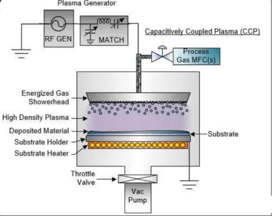
1. Vacuum and pressure control system composition: Mechanical pumps, molecular pumps, vacuum valves, vacuum gauges, etc.
Function: To provide a stable vacuum environment for the deposition process, reducing the impact of nitrogen, oxygen, and water vapor on the quality of the film. Dry pumps are used to extract low vacuum to avoid oil contamination of the substrate. Molecular pumps are used to extract high vacuum, which has strong water vapor removal ability and ensures the cleanliness of the reaction chamber.
Importance: Vacuum environment is the foundation of thin film deposition, directly affecting the purity and uniformity of the film.
2. Deposition system components: Radio frequency power supply, water cooling system, substrate heater, etc.
Function: Radio frequency power supply: Ionizes the reactive gas to generate plasma, promoting chemical reactions.
Water cooling system: Provides cooling for the pump and reaction chamber, preventing equipment overheating and triggering an alarm in case of overtemperature. The cooling water pipes use insulating materials to avoid electrical interference. Substrate heater: Heats the substrate to remove surface impurities and improve the adhesion between the film and the substrate.
Importance: The deposition system is the core of thin film deposition, directly affecting the quality and performance of the film.
3. Gas and flow control system components: Gas cylinders, gas cabinets, mass flow meters, gas delivery pipelines, etc.
Function:
- Gas source: Reactive gases (such as silane, ammonia, nitrogen, etc.) are provided by gas cylinders.
- Gas delivery: The gas is delivered to the process chamber through a gas cabinet.
(3) Flow control: Mass flow meters are used to precisely control the gas flow, ensuring the ratio and stability of the reactive gas flow.
Importance: Gas flow control directly affects the composition, thickness, and uniformity of the film.
4. Reaction chamber system components: Reaction chamber, substrate tray, gas distributor, electrodes, etc.
Function:
(1) Reaction chamber: Provides the reaction space for thin film deposition, usually made of high-temperature and corrosion-resistant materials.
(2) Substrate tray: Fixes the substrate and ensures uniform heating.
(3) Gas distributor: Enables uniform distribution of the reactive gas, ensuring the uniformity of the thin film deposition.
(4) Electrodes: In PECVD processes, used to generate plasma.
Importance: The reaction chamber is the core area of thin film deposition; its design directly affects the quality and performance of the film.
5. Control system components: PLC (Programmable Logic Controller), sensors, human-machine interface ( HMI ), etc.
Function:
(1) Automated control: Through PLC achieves automated operation of various equipment systems.
(2) Parameter monitoring: Real-time monitoring of key parameters such as temperature, pressure, and gas flow.
(3) Fault alarm: Triggers an alarm and automatically shuts down in abnormal situations.
Importance: The control system ensures stable equipment operation, improving process consistency and reliability.
6. Cleaning and maintenance system components: Cleaning gases (such as NF₃ 、 CF₄ ), cleaning pipelines, exhaust gas treatment equipment, etc.
Function:
(1) Chamber cleaning: Regularly removes deposits in the reaction chamber to prevent contamination.
(2) Exhaust gas treatment: Treats harmful gases generated during the reaction process to ensure environmental protection and safety.
Importance: The cleaning and maintenance system extends equipment life and ensures the stability and consistency of thin film deposition.
IV. Thin Film Deposition Equipment International Market
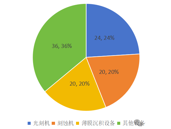
In semiconductor manufacturing equipment, lithography machines, etching machines, and thin film deposition equipment are the three major pieces of equipment. According to SEMI estimated data, lithography machines, etching machines, and thin film deposition equipment respectively account for approximately 24%、20% and 20%。
Thin film deposition equipment is one of the three core equipment in semiconductor production lines; its market size will continue to grow with the advancement of process technology.
2022 year, the global thin film deposition equipment market size was approximately 200 US dollars. It is expected that by 2026 year, the market size will grow to 300 US dollars ,the compound annual growth rate ( CAGR ) is approximately 8-10% 。
Growth driving factors:
1. Advanced process requirements: As semiconductor process technology evolves to 3nm、2nm and below nodes, the number and complexity of thin film deposition processes have greatly increased. For example, 3nm process thin film deposition processes have increased by 90nm times compared to 2.5 process.
2. Storage chip upgrades: From 2D NAND to 3D NAND development, the number of thin film deposition layers has increased significantly. 3D NAND The number of stacked layers has increased from 32 layers to 200 layers or more, leading to a surge in demand for thin film deposition equipment.
3. New emerging applications are driving growth: 5G The growing demand for high-performance chips driven by emerging technologies such as artificial intelligence, the Internet of Things, and autonomous driving is expanding the thin-film deposition equipment market.
4. Market Share Breakdown : CVD Equipment: accounts for approximately 60% of the thin-film deposition equipment market, representing the largest segment. PVD Equipment: accounts for approximately 25%。 ALD Equipment: accounts for approximately 15% However, it is the fastest-growing segment, and it is expected that in the next five years it CAGR will exceed 15%。
Disclaimer:
Parts of this article are reproduced from the internet. The copyright and responsibility for the content belong to the original author. If you are the original author and do not wish to be reproduced, please contact us (sales@hitsemi.com).
News Center
TSV Technology: A Core Pillar of AI Computing Power

Contact: Miss Dai
Address: 1704, Building 1, Chongwen Park, Nanshan Zhiyuan, 3370 Liuxian Avenue, Nanshan District, Shenzhen City, Guangdong Province
Shenyang Office Address: Shenyang University Science Park, No.15 Wanghua South Street, Dadong District, Shenyang City, Liaoning Province
Telephone:13632750017
E-mail:sales@hitsemi.com

Message