Features and functional advantages of plasma coating instrument


Release time:

2024-08-12

Plasma coating instrument is a kind of surface treatment equipment, which has a wide range of applications and important functional advantages. It is mainly used for surface coating and modification treatment. By exposing the material to a plasma environment, the modification and coating of the material surface can be achieved by utilizing the mechanisms of ion bombardment and reactive deposition. This technology has a wide range of applications in various industries, such as electronics, optoelectronics, medical, automotive and other fields.

Plasma coating instrument is a kind of surface treatment equipment, which has a wide range of applications and important functional advantages. It is mainly used for surface coating and modification treatment. By exposing the material to a plasma environment, the modification and coating of the material surface can be achieved by utilizing the mechanisms of ion bombardment and reactive deposition. This technology has a wide range of applications in various industries, such as electronics, optoelectronics, medical, automotive and other fields.

Secondly, the plasma coating instrument has superior functional advantages. It can improve the performance of the material surface. By controlling the ion energy and flow rate in the plasma, the hardness, wear resistance and corrosion resistance of the material can be enhanced, thereby improving the service life and performance stability of the material. Nanoscale coating of the material surface can be achieved. By adjusting the composition of the reaction gas and the deposition conditions, a uniform and dense coating can be formed on the surface of the material, which has excellent optical, electrical and thermal properties. The surface composition of the material can also be adjusted. For example, in the field of optoelectronics, the performance of the semiconductor device can be adjusted by depositing a doped layer.
In addition, the plasma coating instrument also has the characteristics of high efficiency and environmental protection. Compared with the traditional coating technology, the plasma coating instrument can be used to treat the surface of the material at a lower temperature, reducing energy consumption and heat loss. At the same time, the technology does not require the use of harmful solvents and chemicals and is environmentally friendly.
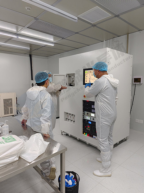
Equipment Manufacturer-Pengcheng Semiconductor Technology (Shenzhen) Co., Ltd
Disclaimer:
Part of this article is reproduced from the Internet, and its copyright and responsibility belong to the original author. If you are the original author and do not want to be reproduced, please contact us (sales@hitsemi.com).


News Center

The TGV glass through-hole technology has achieved a significant breakthrough, and its application prospects continue to expand.

Recently, TGV (Through Glass Via) technology has made significant strides in the fields of materials processing and micro- and nano-manufacturing, drawing considerable attention from the semiconductor, advanced packaging, and emerging electronic device industries. With its outstanding electrical performance, high-frequency characteristics, and three-dimensional integration capabilities, TGV is emerging as one of the key technologies for next-generation high-density interconnects.

Application of TGV Glass Through-Hole Technology in Magnetron Sputtering

As an advanced micro- and nano-fabrication technique, TGV glass via-hole technology has demonstrated tremendous application potential in the field of magnetron sputtering. By precisely fabricating vias on glass substrates, this technology not only enables vertical interconnections for three-dimensional circuits but also significantly enhances the integration and performance of electronic devices.

Diamond: Possessing potential that surpasses existing semiconductor materials, with broader application prospects in the future.

Diamond is used as a semiconductor material—and some scholars even hail it as the “ultimate semiconductor material” and the “ultimate room-temperature quantum material”—owing to its unique physical and chemical properties. Diamond is an ultra-wide-bandgap semiconductor that boasts exceptional electrical, optical, mechanical, thermal, and chemical characteristics. These properties give diamond broad application prospects in numerous fields.

Pengcheng Semiconductor: The Strategy, Tactics, and Survival Guide of a High-Tech Enterprise

The 15th China International Nanotechnology Industry Expo (referred to as "Nanobio"), held under much anticipation, successfully came to a close. This year's event featured one keynote speech, 15 parallel forums, and hosted 605 cutting-edge presentations. Additionally, it included an innovation and entrepreneurship competition, along with three supply-and-demand matchmaking sessions. The expo brought together over 150 nationally recognized talents and more than 500 top experts from leading universities, research institutions, and corporate organizations both domestically and internationally. With an exhibition area spanning 25,000 square meters, the event attracted over 350 of the world's premier companies and institutions, showcasing more than 2,400 of the latest nanotechnology products and innovative applications globally. Over the three-day period, the expo drew nearly 27,500 attendees in total, making it the largest-ever edition in terms of scale and cementing its growing influence on the global stage.

Pengcheng Semiconductor Debuts at the High-End Professional Exhibition on "Optoelectronics + Semiconductors"—Shenzhen's 26th China International Optoelectronic Exposition

When the "light-speed" innovation of optoelectronics meets the "subtle" breakthroughs in semiconductors, two premier, high-end professional exhibitions leading global industry collaboration are set to make a cross-industry debut, shining brightly in Shenzhen. On September 10, the 26th China International Optoelectronic Expo (CIOE China Optics Expo) and SEMI-e Shenzhen International Semiconductor Exhibition, along with the 2025 Integrated Circuit Industry Innovation Expo, unveiled themselves at the Shenzhen International Convention & Exhibition Center. With an exhibition space exceeding 300,000 square meters, attracting over 5,000 exhibitors and expected to draw 160,000 professional visitors, these events have established a new benchmark for collaborative development between the optoelectronics and semiconductor industries, injecting powerful momentum into the global tech sector as it breaks through technological barriers and sparks fresh waves of innovation.