 Co.,Ltd.")

The use of magnetron sputtering coating instrument and matters needing attention
Release time:
2024-07-29


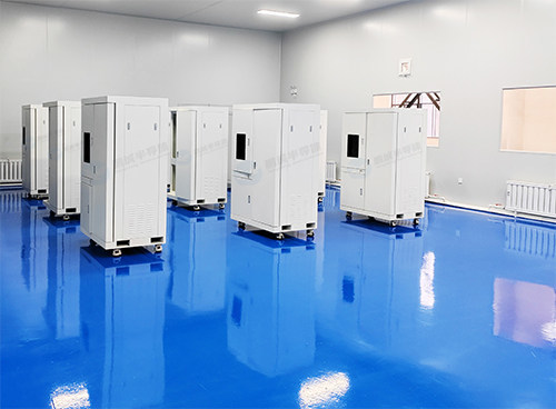
Magnetron sputtering coating instrument (PVD coating equipment) is a common surface coating equipment. It is a technology that uses evaporation or sputtering to deposit thin films on the surface of a substrate under vacuum conditions to prepare metals, alloys, compounds, semiconductors, ceramics, dielectric composite films and other chemical reaction films. It is suitable for plating various single-layer films, multi-layer films, doped films and alloy films, and can be used for plating magnetic materials and non-magnetic materials. Widely used in electronics, optoelectronics, optics, medical and other industries. In order to ensure its normal use and obtain a good coating effect, the following are some details and techniques that need to be paid attention to when using the magnetron sputtering coating instrument.
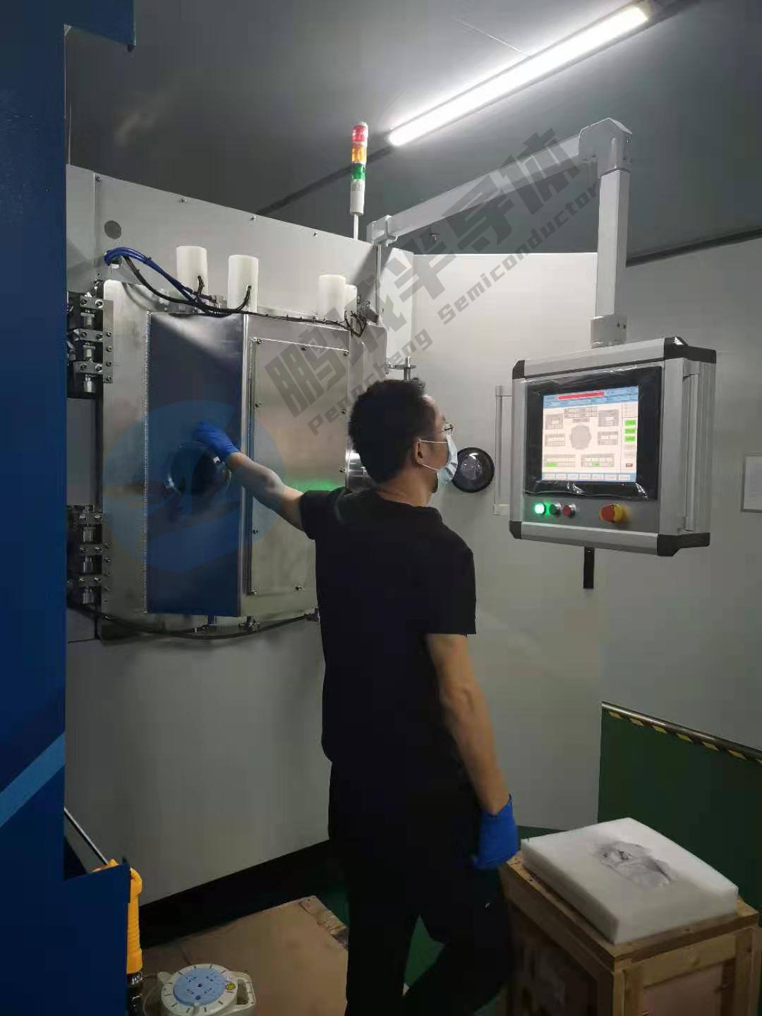
Correct installation and commissioning of the magnetron sputtering coater is an important step to ensure its normal operation. During the installation process, it is necessary to ensure the stability of the equipment and avoid excessive vibration and force. During debugging, the operation must be carried out in accordance with the requirements of the operation manual, and the parameters and key components must be adjusted to ensure that the equipment can achieve the expected performance indicators.
The vacuum system of the magnetron sputtering coating instrument needs to be fully evacuated before use and maintain a good sealing state. The evacuation process of the vacuum system takes a period of time, usually several hours or even longer. After the vacuum extraction is completed, the vacuum system should be tested for tightness to ensure that there are no obvious air leaks.
The selection and preparation of coating materials is also very important. When choosing a coating material, you need to consider the characteristics and requirements of the object to be coated, and choose the appropriate material. In the process of preparing the material, it is necessary to ensure that the material is of high purity, the particles are fine and uniform, and necessary cleaning treatment is carried out to ensure the quality and purity of the material.
When operating the magnetron sputtering coater, pay attention to the following points. To avoid device overheating and overload. According to the characteristics and requirements of the coating material, reasonably adjust the power, current and working time and other parameters to avoid overheating causing material melting or equipment damage. To follow the operating procedures, the correct use of coating process and procedures to ensure the uniformity and consistency of the coating.

Regular inspection and maintenance of magnetron sputtering coater is also very important. Regularly check the various components and key parameters of the equipment, find and solve problems in time to ensure the stability and reliability of the equipment. At the same time, do a good job of cleaning the equipment, keep the equipment clean and tidy, and avoid the influence of impurities and pollutants on the coating effect.
Equipment Manufacturer-Pengcheng Semiconductor Technology (Shenzhen) Co., Ltd
News Center
TSV Technology: A Core Pillar of AI Computing Power

Contact: Miss Dai
Address: 1704, Building 1, Chongwen Park, Nanshan Zhiyuan, 3370 Liuxian Avenue, Nanshan District, Shenzhen City, Guangdong Province
Shenyang Office Address: Shenyang University Science Park, No.15 Wanghua South Street, Dadong District, Shenyang City, Liaoning Province
Telephone:13632750017
E-mail:sales@hitsemi.com

Message