 Co.,Ltd.")

.jpg")
MBE molecular beam epitaxy equipment
Molecular Beam Epitaxy (MBE) thin-film growth equipment—Molecular Beam Epitaxy MBE—enables epitaxial growth on certain substrates, allowing for the fabrication of molecular self-assembled structures, superlattices, quantum wells, one-dimensional nanowires, and more. It can also be used for process verification and the growth and fabrication of epitaxial wafers for both second-generation and third-generation semiconductors. During thin-film epitaxial growth, Molecular Beam Epitaxy equipment provides an ultra-high vacuum environment, enabling epitaxial growth under ideal conditions. This eliminates various interfering factors during film growth, resulting in high-precision thin films with exceptional accuracy.
- Product Description
-
Molecular Beam Epitaxy Thin-Film Growth Equipment (MBE) (Molecular Beam Epitaxy MBE) This equipment enables epitaxial growth on certain substrates, allowing for the fabrication of molecular self-assembled structures, superlattices, quantum wells, and one-dimensional nanowires. It can also be used for process verification of second-generation and third-generation semiconductors, as well as for the growth and fabrication of epitaxial wafers.
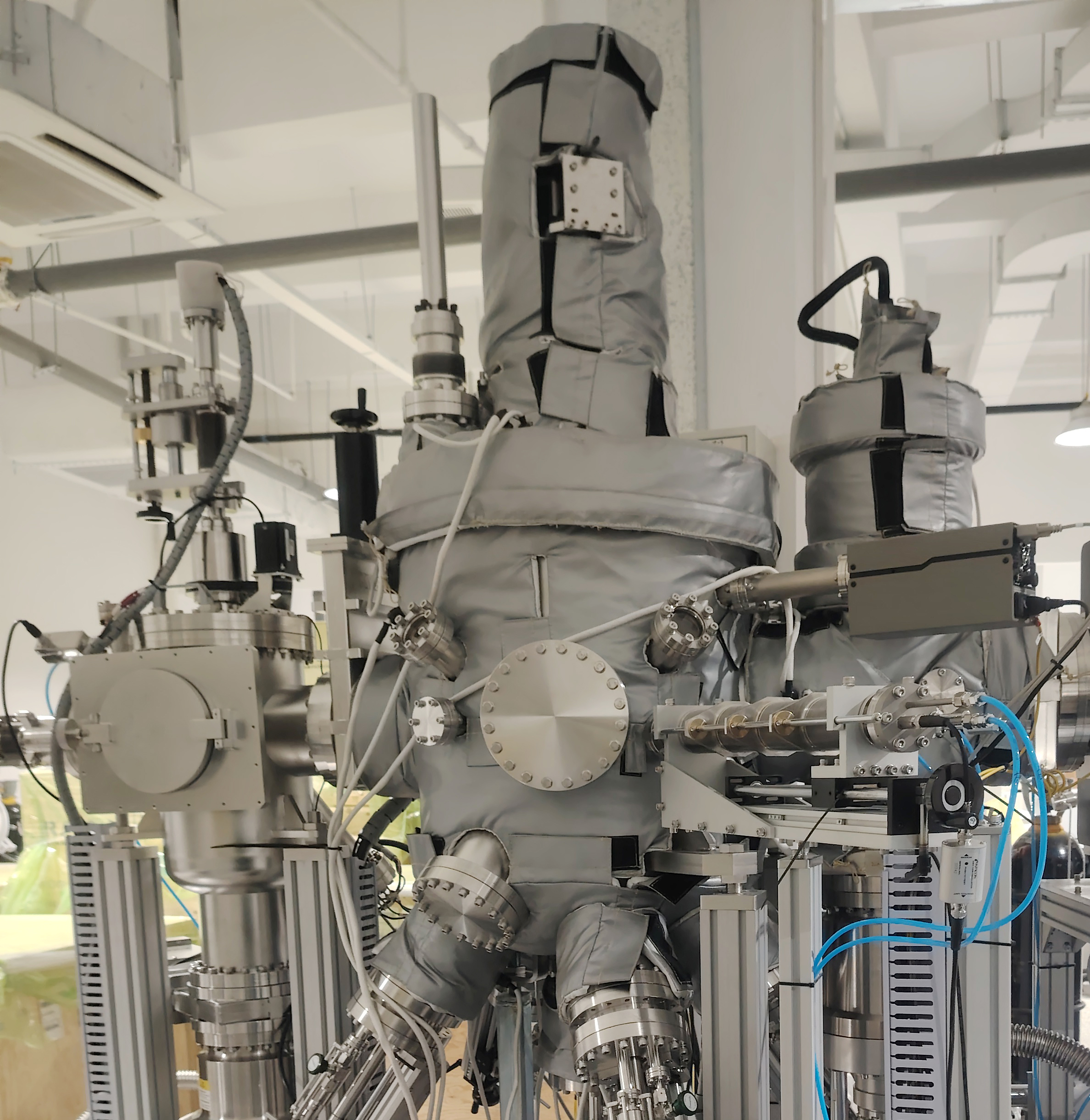
Molecular beam epitaxy (MBE) thin-film growth equipment features an ultra-high vacuum environment during thin-film epitaxial growth, enabling epitaxial film growth under ideal conditions. This allows the system to eliminate various interfering factors that might otherwise affect film growth, thus producing high-precision thin films with exceptional accuracy.
The molecular beam epitaxy thin-film growth experimental equipment designed and manufactured by our company comes in two types: experimental and production models. It features a reasonable configuration, a simple structure, convenient operation, advanced technology, reliable performance, versatile applications, strong practicality, and a relatively low price. It is suitable for use in university laboratories and research institutions as teaching experiments, scientific research, and process development in the field of molecular beam epitaxy.Production-oriented MBE can be used for the preparation of small-batch epitaxial wafers.
Functional Features
In 2005, this project was the first in China to complete the R&D, design, and manufacturing of a fully domestically produced MBE system, achieving independent control and controllability.
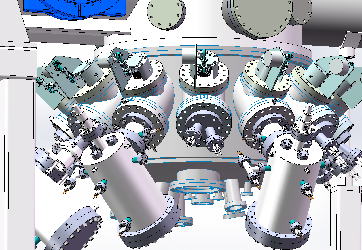
Core components include an independently designed MBE ultra-high vacuum epitaxial growth chamber, process control system and software, RHEED in-situ real-time online monitoring instrument, linear electron gun, high-temperature beam source furnace, beam source furnace power supply, high-temperature sample stage, and film thickness meter (capable of measuring the number of molecular layers grown epitaxially).
It enables epitaxial growth of both second-generation semiconductors (such as gallium arsenide) and third-generation semiconductors (such as silicon carbide and gallium nitride).
After more than two decades of process exploration and continuous equipment upgrades, we have now developed the capability to design, manufacture, and produce commercial MBE equipment. Our equipment features a rational configuration, a simple structure, advanced technology, reliable performance, versatile applications, strong practicality, and an excellent price-to-performance ratio.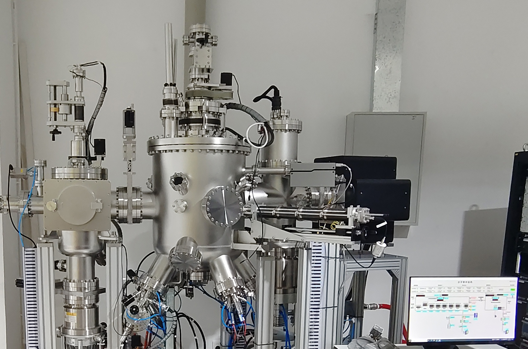
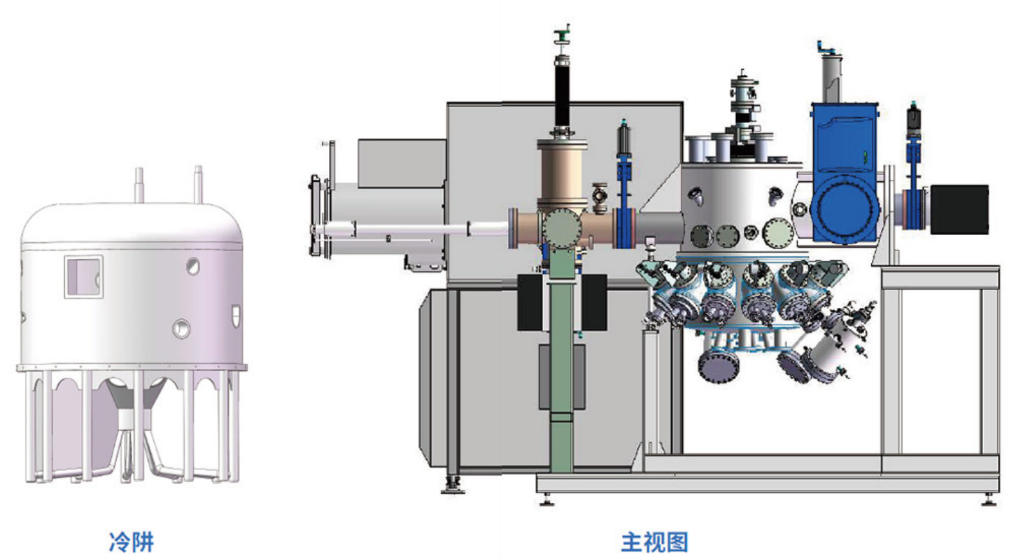
Equipment Composition and Main Technical Specifications
The composition of the device
Sample injection chamber
This room is used for the storage and retrieval of samples and is equipped with a multi-disc storage function. The sample library can hold six substrate wafers.
Preprocessing Room
This chamber is used for vacuum plasma stripping and vacuum high-temperature degassing of samples prior to their entry into the epitaxy chamber, as well as for other preliminary process treatments. It is also used for post-processing of epitaxially grown wafers, such as high-temperature annealing and other similar procedures.
Extension Room
Ultra-high vacuum clean vacuum chamber, enabling molecular beam epitaxy processes.
Main Technical Specifications of Molecular Beam Epitaxy (MBE) Thin-Film Growth Equipment (Molecular Beam Epitaxy MBE)
Sample injection chamber
Ultimate vacuum: 5.0 × 10 -5 Pa
Sample loading quantity: 6 pieces
Preprocessing Room
Ultimate vacuum: 5×10 -7 Pa
Sample stage heating temperature: Room temperature to 850℃ ± 1℃ (PID control)
Ion cleaning source: Φ60; 100–500 eV
Extension RoomProject
Parameter
Extreme vacuum Ion pump 8.0 × 10 -9 Pa (cold trap-assisted) / cryopump Sample stage heating temperature Room temperature to 1200℃ ±1℃ (PID control) Sample rotation speed 2 to 20 RPM (continuously adjustable) Gaseous ionization source 1–2 sets (nitrogen) Solid-state beam source furnace 3 to 10 sets (configured according to user requirements) Rheed 1 set *Some components in the process room vary depending on customer requirements.
Experimental MBE (Single Substrate)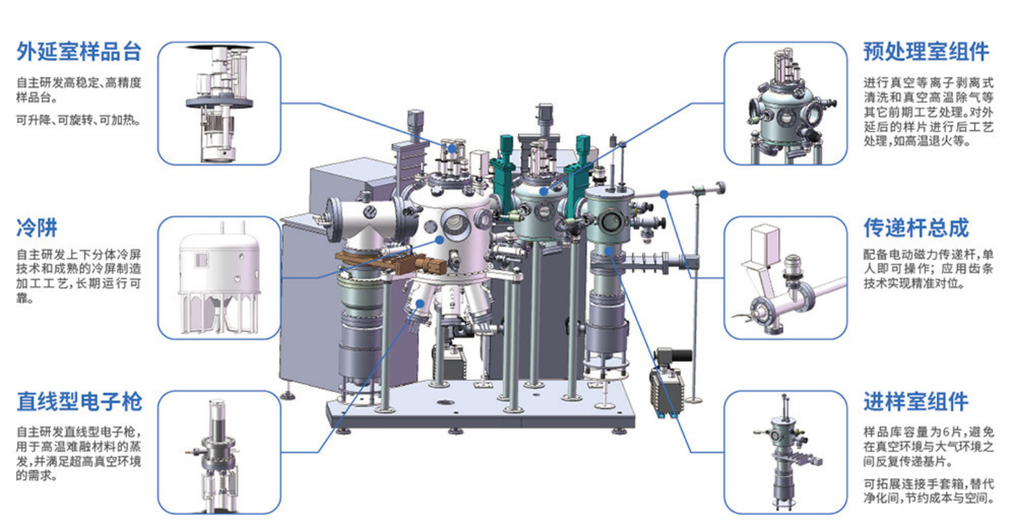
Device components
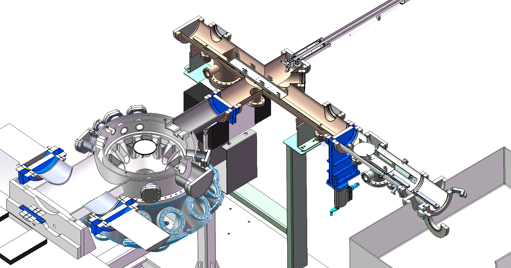
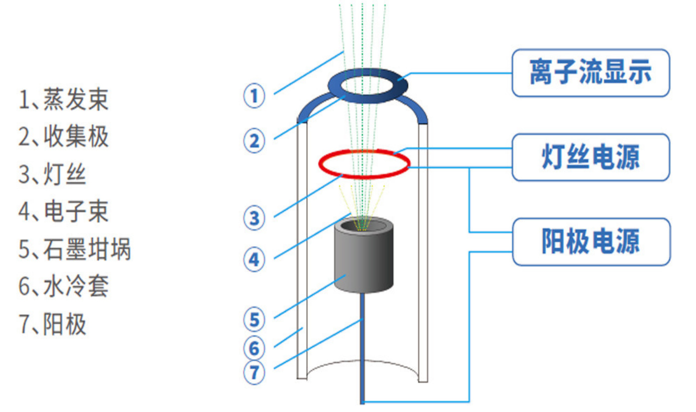
Ultra-high vacuum linear electron gun
Independently developed linear electron gun that meets the requirements for ultra-high vacuum and flange interfaces as well as installation dimensions of beam-source furnaces; it can be used for the heating and evaporation of high-temperature, refractory materials.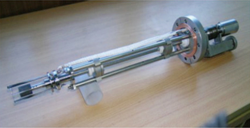
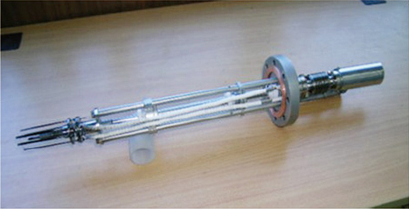
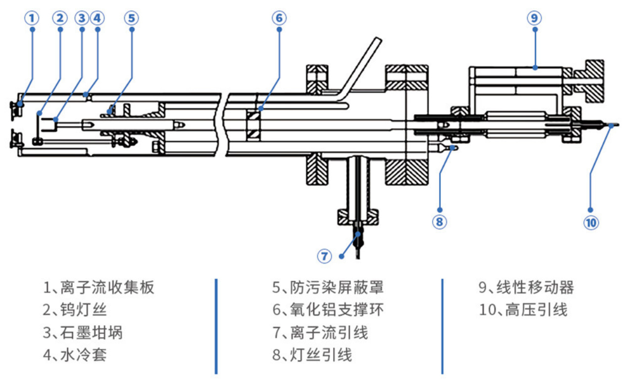
Ultra-high vacuum linear electron gun
High-energy diffraction gun and power supply
Spot size: 0.6 mm, high voltage: 25 kV.
The light spot on the fluorescent screen can diffract an image, which is then captured by a CCD camera and processed by a computer.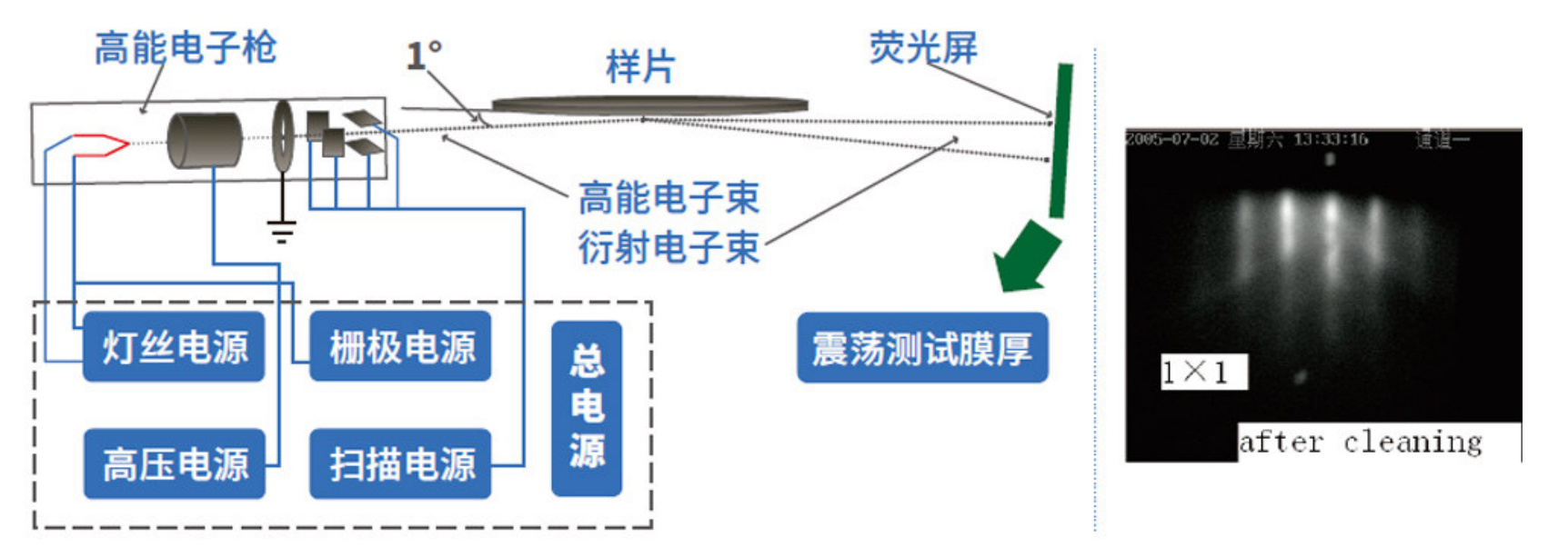
Production-oriented MBE (large-size single substrate, multiple small-size substrates)
Process Implementation
Bi grown using the molecular beam epitaxy equipment independently developed by Pengcheng Semiconductor. 2-x Sb x You 3。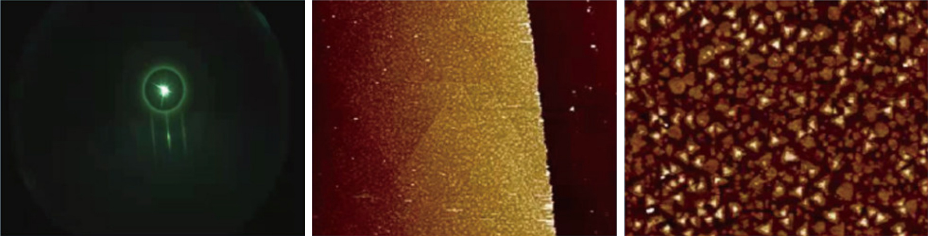
Key words:
Get Quote
Related Products
")
 HITSemi-PVD-650SR")


Contact: Miss Dai
Address: 1704, Building 1, Chongwen Park, Nanshan Zhiyuan, 3370 Liuxian Avenue, Nanshan District, Shenzhen City, Guangdong Province
Shenyang Office Address: Shenyang University Science Park, No.15 Wanghua South Street, Dadong District, Shenyang City, Liaoning Province
Telephone:13632750017
E-mail:sales@hitsemi.com

Message