

Pengcheng Semiconductor invites you to attend the SEMI-e 2024 Shenzhen International Semiconductor Exhibition from June 26 to 28 at Shenzhen International Convention and Exhibition Center (Bao 'an)
Release time:
2024-06-17


The 6th Shenzhen International Semiconductor Exhibition SEMl-e2024 will be held in Shenzhen International Convention and Exhibition Center (Baoan) from June 26 to 28. As an influential and representative industry event in the semiconductor field, this exhibition will bring together more than 800 exhibitors to display chip design, wafer manufacturing and packaging, semiconductor special equipment and parts, advanced materials, third-generation semiconductors/IGBTs, The semiconductor industry chain dominated by automotive semiconductors will build a new ecology of semiconductor industry exchange and integration.
Pengcheng Semiconductor Technology (Shenzhen) Co., Ltd. (referred to as: Pengcheng Semiconductor), which focuses on the R & D, design and manufacturing of micro-nano materials (including semiconductor materials), micro-nano manufacturing process and micro-nano equipment, is a supplier. With the help of SEMl-e2024, a platform for displaying innovative technology products and applications, pengcheng Semiconductor will exhibit its carefully developed HFCVD hot filament chemical vapor deposition system solutions, scientific research/production magnetron sputtering (PVD vacuum coating) solutions, molecular beam epitaxial film growth equipment MBE, PECVD plasma enhanced chemical vapor deposition solutions, etc. We are looking forward to guests from home and abroad to visit booth 4B39, Hall 4, Shenzhen International Convention and Exhibition Center (Baoan) to jointly explore new paths for the development of the semiconductor industry, seek new opportunities for the industry, and jointly write a new chapter in the high-quality development of the industry.
The HFCVD hot filament chemical vapor deposition system solution can be used for the production of micron crystal and nanocrystalline diamond wafers, as well as anti-corrosion and wear-resistant hard coatings, diamond BDD electrodes, solar thin film cells, etc.

Independent research and development and production of single/double coated hot filament CVD diamond equipment (HFCVD) can prepare diamond polycrystalline wafer substrate size: 2 inches, 4 inches, 6 inches, 8 inches.
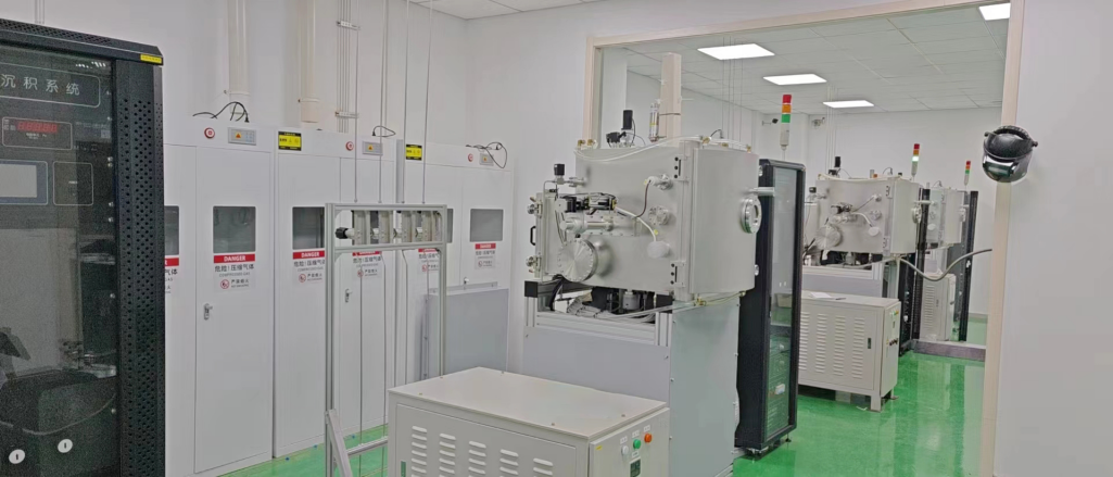
Diamond film production line
Application areas: third-generation semiconductors, high-power lasers, 10G communications, micro-nano acoustics, power amplifiers, filter devices, etc.; can be used for the development and production of diamond products of mechanical, thermal, optical and acoustic levels.
Scientific research/production magnetron sputtering solutions: vacuum conditions using evaporation or sputtering deposition of thin films on the surface of the substrate technology, the preparation of metals, alloys, compounds, semiconductors, ceramics, dielectric composite film and other chemical reaction film, suitable for plating a variety of single-layer film, multilayer film, doped film and alloy film, can be plated magnetic materials and non-magnetic materials.
The magnetron sputtering thin film deposition technology, upgrade to thin film epitaxy technology, for the domestic initiative. The breakthrough of this technology makes the device expected to be applied in the epitaxial process of the third generation semiconductor GaN and the fourth generation semiconductor Ga2O3.

Multi-source large-size MBE device solutions can realize epitaxial growth processes on certain substrates, realize molecular self-assembly, superlattices, quantum wells, one-dimensional nanowires, etc. Process verification of second-generation semiconductors and third-generation semiconductors and growth fabrication of epitaxial wafers can be performed.
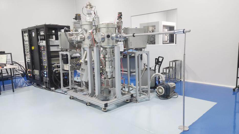
The molecular beam epitaxy thin film growth equipment MBE has an ultra-high vacuum environment during thin film epitaxial growth, which is an ideal environment for thin film epitaxial growth, which can eliminate various interference factors during thin film growth and obtain ideal high-precision thin films.

PECVD Plasma Enhanced Chemical Vapor Deposition Solutions
PECVD plasma enhanced chemical vapor deposition equipment is mainly used for silicon nitride and silicon oxide film growth in a clean vacuum environment; using single-frequency or dual-frequency plasma enhanced chemical vapor deposition technology, it is an ideal process equipment for depositing high-quality silicon nitride, silicon oxide and other thin films.
Domestic products should be leading (dual-band technology)

From June 26 to 28, the 6th Shenzhen International Semiconductor Exhibition in SEMl-e 2024 is about to open. We look forward to and warmly invite all guests to visit Pengcheng Semiconductor booth to explore innovative achievements in the field of semiconductor equipment and materials, discuss new technologies, new products and new trends in the development of the industry, and jointly promote the upgrading development of the industrial chain.
The 6th Shenzhen International Semiconductor Exhibition SEMI-e
We look forward to seeing you
26-28 June
Shenzhen International Convention and Exhibition Center (Baoan New)-Hall 4 4B39
Waiting for you
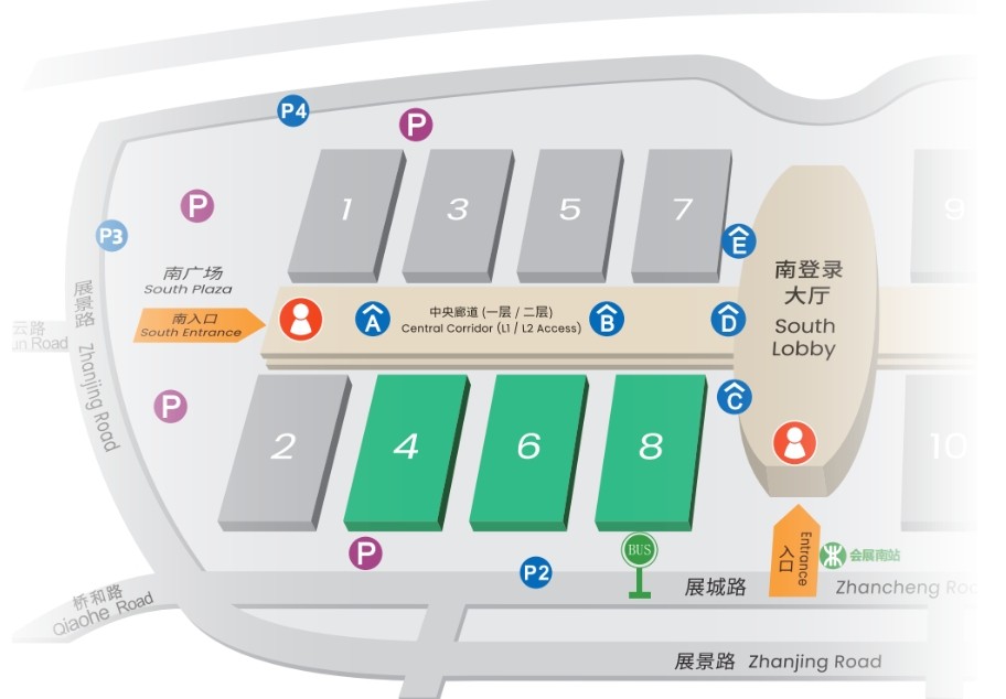
Traffic Guidelines: Exit C1/C2 of Metro Line 12/Line 20 National Exhibition Station reaches the South Login Hall of the Exhibition Hall.
Company Profile:
Pengcheng Semiconductor Technology (Shenzhen) Co., Ltd. was jointly initiated by Harbin Institute of Technology (Shenzhen) and a team of engineers with many years of practical experience. Based on the intersection of market frontier, industry frontier and technology frontier, the company seeks innovation guidance and sustainable development, solves the pain points of the industry and the problem of localization, and strives for the independent control of the industrial chain.
The company's core business is micro-nano materials (including semiconductor materials), micro-nano manufacturing process, micro-nano equipment research and development design and manufacturing.
Scientific research equipment: PVD, CVD, MBE molecular beam epitaxy, etc.
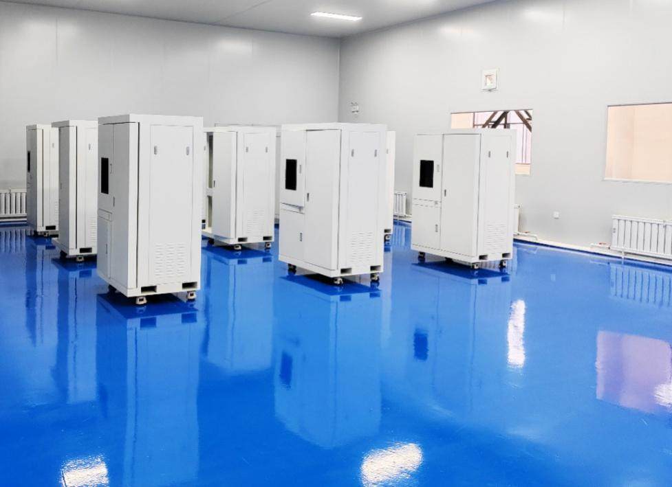
Industrial production equipment: large-scale evaporation equipment, multi-arc ion source coating equipment, rectangular magnetron sputtering coating equipment, electron beam evaporation equipment, OLED coating equipment, HFCVD hot wire chemical vapor deposition equipment, vacuum high temperature CVD furnace, six-inch MBE production equipment.
The company's technology and products can be widely used in: new materials, new energy, microelectronics, optoelectronics, semiconductors, acoustics, optics, micro-electromechanical systems (MEMS); sensors, biomedicine, precision medicine, health, environmental protection, micro-nano robots, Surface technology and other fields.
The company's core R & D team has a complete knowledge structure, including a high-level material research and process research team with professors and doctors of Harbin Institute of Technology as the core, as well as a team of senior equipment designers from the industry. The company team has more than 20 years of experience in micro-nano materials and device research (including semiconductor materials), PVD/CVD deposition technology research, epitaxial technology research, thin film preparation equipment design and manufacturing.
News Center
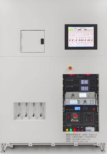
Thin film deposition equipment

Contact: Miss Dai
Address: 1704, Building 1, Chongwen Park, Nanshan Zhiyuan, 3370 Liuxian Avenue, Nanshan District, Shenzhen City, Guangdong Province
Shenyang Office Address: Shenyang University Science Park, No.15 Wanghua South Street, Dadong District, Shenyang City, Liaoning Province
Telephone:13632750017
E-mail:sales@hitsemi.com

Message