

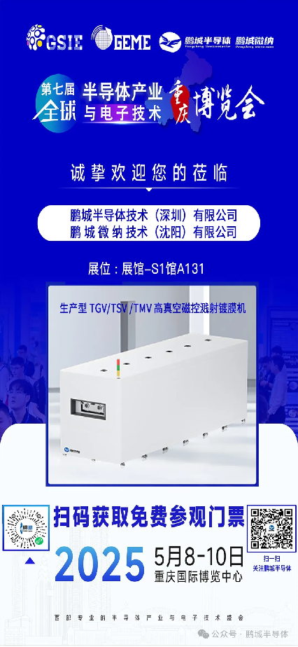
Exhibition Invitation | Pengcheng Semiconductor sincerely invites you to attend the 7th Global Semiconductor Industry (Chongqing) Expo
Release time:
2025-04-24


The 7th Global Semiconductor Industry (Chongqing) Expo will be held at the Chongqing International Expo Center from May 8th to 10th, 2025. The theme of the expo is "New Era, Creating a Smart Future." It will feature an exhibition area of 40,000㎡, 800 exhibiting companies, and attract 35,000 professional visitors for visits and exchanges.
Pengcheng Semiconductor will showcase its cutting-edge thin-film deposition equipment and technical solutions at booth S1-A131. Based on nano and atomic manufacturing PVD/CVD technology, it is used for high-quality film preparation. For example, using magnetron sputtering technology for single-crystal thin film preparation, and using magnetron sputtering as the beam source for molecular beam epitaxy. Exhibits cover popular application areas such as micro-nano optics, acoustics, and medical fields. This 7th Global Semiconductor Industry (Chongqing) Expo will bring cutting-edge technologies and product debuts. We sincerely invite all new and old customers to visit our booth for discussions and exchanges!
Company Introduction
Pengcheng Semiconductor Technology ( Shenzhen ) Co., Ltd., jointly initiated and established by Harbin Institute of Technology ( Shenzhen ) and an engineer team with years of practical experience. The company is based on the intersection of technological and market frontiers, seeking innovation leadership and sustainable development, solving industry pain points and localization problems, and striving for independent and controllable industrial chains.
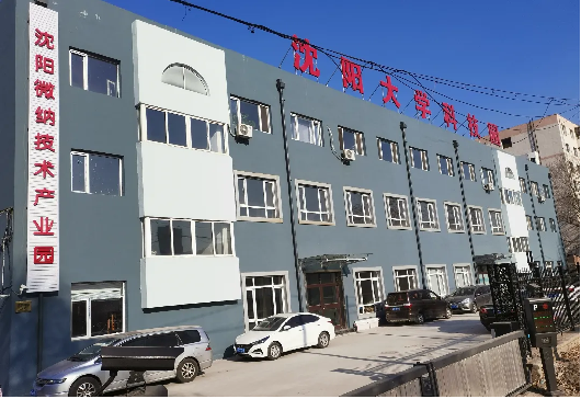
Pengcheng Micro-Nano Technology (Shenyang) Co., Ltd. is a wholly-owned subsidiary of Pengcheng Semiconductor Technology (Shenzhen) Co., Ltd., serving as the design center and production base for semiconductor processes and equipment.
The company's core business is micro-nano technology and high-end precision manufacturing. Specific application areas include the R&D, design, production, manufacturing, and process technology services of semiconductor materials, semiconductor processes, and semiconductor equipment, as well as the upgrading and transformation of semiconductor equipment. We can provide process R&D and prototyping for users.
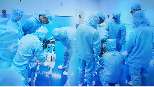
The company's talent team has a complete knowledge structure, with a high-level material research and process research team led by professors and doctors from Harbin Institute of Technology; there is also a senior equipment designer team from the industry, who have 20 years of experience in semiconductor material research, epitaxial technology research, and the design, production, and manufacturing of complete sets of semiconductor thin-film preparation equipment.
The company relies on Harbin Institute of Technology ( Shenzhen ) and has advanced semiconductor R&D equipment platforms and testing equipment platforms, enabling high-starting-point scientific research. The company's headquarters is located in Shenzhen and has the capability for R&D, production, debugging of semiconductor equipment, as well as pilot testing, production, and sales of semiconductor materials and devices.
Product Introduction
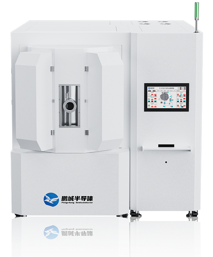
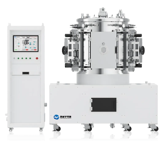
1 Production-type TGV/TSV/TMV High Vacuum Magnetron Sputtering Coating Machine
Production-type TGV/TSV/TMV High Vacuum Magnetron Sputtering Coating Machine (Sputter-2000W series) This equipment is used for coating high-density through-holes and blind holes on glass and ceramic substrates with an aspect ratio >10:1. For example, it is used in the substrate coating process for Cu/Ti microstructure and Au/TiW transmission line dual-system film deposition, providing support for increasing the density of microsystem integration. Advantages of this equipment: high film uniformity and repeatability, strong film adhesion, and programmable automated control based on process formulas.
2 Production-type High Vacuum Magnetron Sputtering / Ion-assisted / Multi-arc Composite Coating Machine
Production-type High Vacuum Magnetron Sputtering / Ion-assisted / Multi-arc Composite Coating Machine ( PVD-1000S series) This equipment is widely used in the preparation of hard and wear-resistant coatings on the surfaces of milling cutters, drills, bearings, gears, lenses, etc. It integrates workpiece surface treatment, ion cleaning, particle control, magnetron sputtering, ion-assisted coating, and reactive sputtering coating methods into one PVD equipment.
3. HFCVD Diamond Film Preparation Equipment
R&D and manufacturing of hot filament CVD diamond equipment, divided into two categories: experimental equipment and production equipment. The equipment is mainly used for the R&D and production of microcrystalline and nanocrystalline diamond films. It can be used for the R&D and production of diamond products at the mechanical, thermal, optical, and acoustic levels. It can manufacture large-size polycrystalline diamond wafers for use as heat sinks for high-power devices, high-frequency devices, and high-power lasers. It can be used for the production of corrosion-resistant and wear-resistant hard coatings; diamond products used in wastewater treatment in the environmental protection field. It can be used for the preparation of diamond films on flat workpieces, and also for the preparation of diamond hard coatings on the surfaces of tools or other irregular surfaces. It can be used for the R&D and production of thin-film solar cells.
4. High Vacuum Magnetron Sputtering System
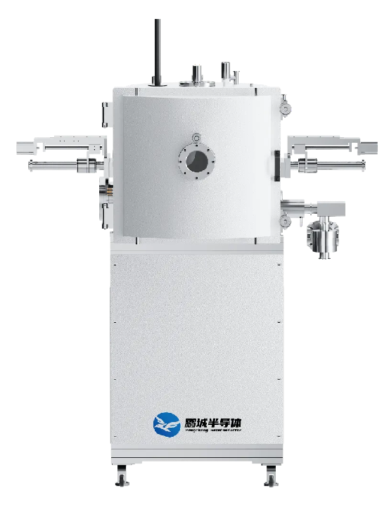
Research-type High Vacuum Magnetron Sputtering Coating Machine Circular Sputter series is our company's research-type high-vacuum magnetron sputtering system. It mainly uses the method of sputtering with a circular magnetron sputtering target to prepare metal, alloy, compound, semiconductor, ceramic, dielectric composite films, and other chemical reaction films; it is suitable for plating various single-layer films, multi-layer films, doped films, and alloy films; it can plate magnetic and non-magnetic materials. It can be used for TGV/TSV/TMV advanced packaging R&D, high aspect ratio ( ≥10:1 ) deep hole seed layer coating.
5 Molecular Beam Epitaxy Thin Film Growth Equipment ( MBE )
Molecular Beam Epitaxy Thin Film Growth Equipment ( MBE Epitaxial growth can be achieved on certain substrates, enabling molecular self-assembly, superlattices, quantum wells, and one-dimensional nanowires. It allows for process verification and epitaxial wafer growth of second and third-generation semiconductors. Molecular beam epitaxy thin film growth equipment provides an ultra-high vacuum environment during thin film epitaxial growth, creating ideal conditions for minimizing interference factors and achieving high-precision films.
Our company designs and manufactures molecular beam epitaxy thin film growth experimental equipment, available in experimental and production models. These models feature reasonable configurations, simple structures, convenient operation, advanced technology, reliable performance, diverse applications, strong practicality, and relatively low prices. They are suitable for use in university laboratories and research institutions for molecular beam epitaxy teaching experiments, scientific research, and process experiments. Production type MBE Can be used for the preparation of batch epitaxial wafers.
6. PECVD Plasma Enhanced Chemical Vapor Deposition
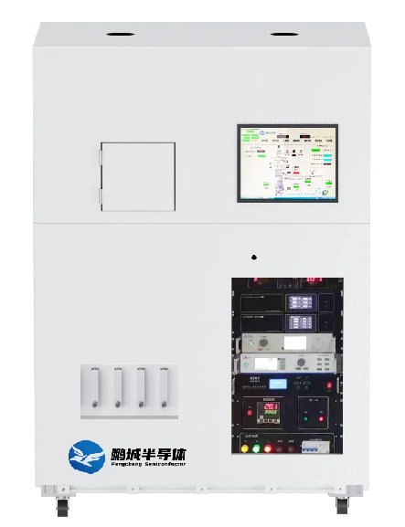
PECVD Plasma Enhanced Chemical Vapor Deposition equipment is mainly used for the growth of silicon nitride and silicon oxide films in a clean vacuum environment. Using single-frequency or dual-frequency plasma-enhanced chemical vapor deposition technology, it is an ideal process equipment for depositing high-quality silicon nitride and silicon oxide films.
7. Production Type High Vacuum Magnetron Sputtering and Ion-Assisted Composite Coating Machine
Production Type High Vacuum Magnetron Sputtering and Ion-Assisted Composite Coating Machine (PVD-1000B series) This equipment uses magnetron sputtering, ion assistance, and reactive sputtering processes to prepare various thin film materials on the surface of workpieces. This equipment integrates workpiece surface treatment, ion cleaning, particle control, magnetron sputtering, ion-assisted coating, and reactive sputtering coating processes into a single PVD device.
7th Global Semiconductor Industry (Chongqing) Expo
Time: May 8-10, 2025
Location: Chongqing International Expo Center
Theme: New Era · Creating a 'Heart' Future
Booth No.: Hall S1 - A131
News Center
Application of TGV Glass Through-Hole Technology in Magnetron Sputtering
Pengcheng Semiconductor: The Strategy, Tactics, and Survival Guide of a High-Tech Enterprise

Contact: Miss Dai
Address: 1704, Building 1, Chongwen Park, Nanshan Zhiyuan, 3370 Liuxian Avenue, Nanshan District, Shenzhen City, Guangdong Province
Shenyang Office Address: Shenyang University Science Park, No.15 Wanghua South Street, Dadong District, Shenyang City, Liaoning Province
Telephone:13632750017
E-mail:sales@hitsemi.com

Message