 Co.,Ltd.")

Pengcheng's semiconductor glass substrate TGV technology supports advanced packaging.
Release time:
2025-02-17


In the field of advanced packaging, whether in 2.5D packaging with interposers or in 3D packaging, TSV is required.TSV, but recently many people have heard the term Through Glass Via (TGV).Through Glass Via (TGV)has great potential and may become a common technology in advanced packaging in the future. This article will briefly describe the application and development trends of Through Glass Via (TGV) in advanced packaging, as well as an overview of the process.
Glass substrates are the next generation of chip substrates, with the core material made of glass. The key technology for glass substrate packaging is TGV. The glass substrate industry chain includes production, raw materials, equipment, technology, packaging, testing, and applications, with upstream being production, raw materials, and equipment. Due to its unique physical and chemical properties, glass substrates show great potential in the application field of electronic component materials.
The global IC packaging substrate market is rapidly developing, and it is expected to reach a scale of 31.54 billion USD by 2029. Glass substrates are the latest trend, with an expected penetration rate of over 50% within five years. The global glass substrate market has vast potential, expected to grow to 11.3 billion USD by 2031. The market size of glass substrates in China is continuously expanding, reaching 33.3 billion CNY in 2023. Domestic manufacturers have significant cost advantages, and the localization of glass substrates is accelerating, providing a huge market space.
The Through-Glass Via (TGV) interconnection technology can be traced back to 2008, derived from the 2.5D/3D integrated TSV adapter board technology, mainly used to solve the problems of high-frequency or high-speed signal transmission degradation caused by silicon substrate loss, high material costs, and complex processes associated with TSV adapter boards.In recent years, the technology has become increasingly refined. Leading companies have begun to layout and produce some samples for different fields, including: sensors, CPUs, GPUs, AI, display panels, medical devices, and advanced semiconductor packaging.
The advantages of Through Glass Via (TGV) are mainly reflected in:
1) Excellent high-frequency electrical characteristics.
2) Large size ultra-thin glass substrates are easy to obtain.
3) Low cost. Benefiting from the easy availability of large size ultra-thin panel glass and the lack of need for depositing insulating layers, the production cost of glass adapter boards is about 1/8 that of silicon-based adapter boards.
4) Simple process flow. There is no need to deposit insulating layers on the substrate surface and the inner walls of TGV, and thinning is not required in ultra-thin adapter boards.
5) Strong mechanical stability. Even when the thickness of the adapter board is less than 100µm, warping remains minimal.
6) Wide application fields, it is an emerging vertical interconnection technology applied in wafer-level packaging, providing a new technical approach for achieving the shortest distance and minimum spacing between chip-to-chip interconnections, with excellent electrical, thermal, and mechanical properties. It has unique advantages in fields such as RF chips, high-end MEMS sensors, and high-density system integration, making it one of the preferred choices for the next generation of 5G and 6G high-frequency chip 3D packaging.
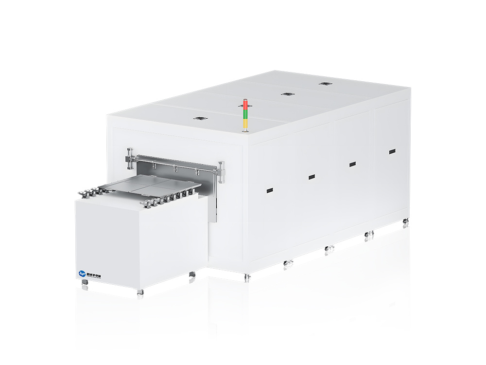
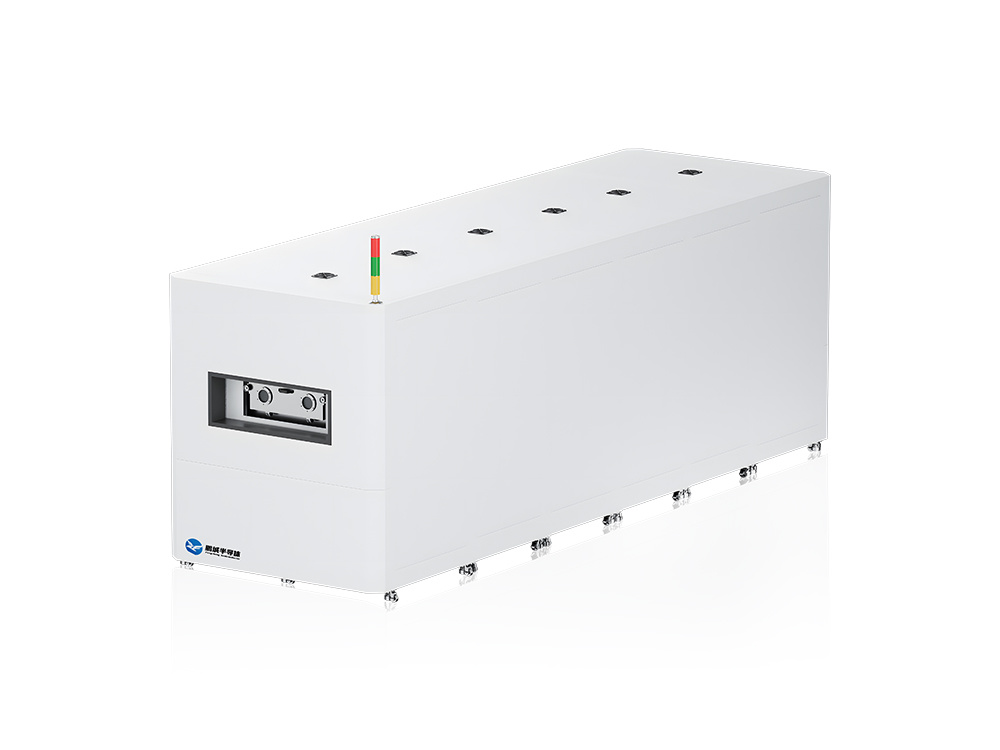
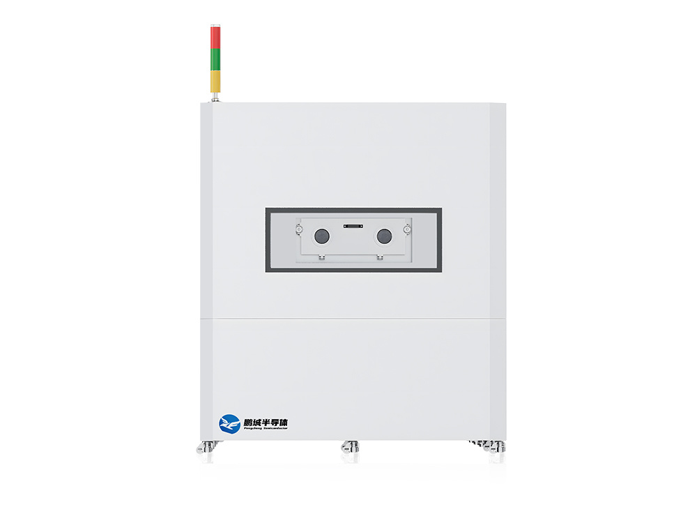
Equipment Manufacturer -Pengcheng Semiconductor Technology (Shenzhen) Co., Ltd.
Disclaimer:
Some parts of this article are reproduced from the internet, and the copyright and responsibility belong to the original author. If you are the original author and do not wish to be reproduced, please contact us for processing (sales@hitsemi.com).
News Center
TSV Technology: A Core Pillar of AI Computing Power

Contact: Miss Dai
Address: 1704, Building 1, Chongwen Park, Nanshan Zhiyuan, 3370 Liuxian Avenue, Nanshan District, Shenzhen City, Guangdong Province
Shenyang Office Address: Shenyang University Science Park, No.15 Wanghua South Street, Dadong District, Shenyang City, Liaoning Province
Telephone:13632750017
E-mail:sales@hitsemi.com

Message