Production-type TGV/TSV


Release time:

2024-12-27

The production-type TGV/TSV high vacuum magnetron sputtering coating machine is used for coating high-density through holes and blind holes on glass substrates and ceramic substrates, with a depth-to-diameter ratio greater than 10:1. For example, it is used for the substrate coating process of Cu/Ti microstructures and the deposition capability of Au/TiW transmission line dual system films, providing support for the enhancement of micro-system integration density.

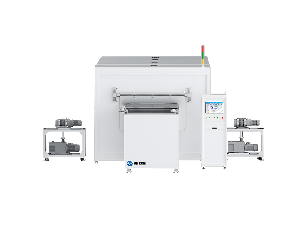
Production-type TGV/TSV high vacuum magnetron sputtering coating machineThis equipmentis used forglass substratesandceramic substratesforhigh-density through holesand blind holes coating, with a depth-to-diameter ratio >10:1. For example: used for substrate coating processes such as Cu/Ti microstructures and Au/TiW transmission line dual system film layer deposition capabilities, providing support for the increase in micro-system integration density.

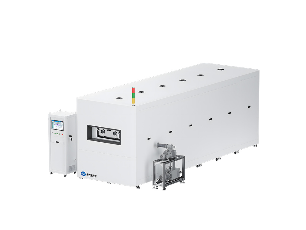
Equipment advantages: high uniformity and repeatability of the film layer, strong adhesion of the film layer, and programmable automated control based on process formulas.

Equipment structure and performance parameters

- Single coating chamber, double coating chamber, multi-chamber coating chamber

- Horizontal structure, vertical structure

- Linear type, cluster type

- Sample transfer: linear type, circumferential type

- Number and type of magnetron sputtering targets: multiple rectangular magnetron targets

- Magnetron sputtering targets: compatible with DC, RF, medium frequency, and high-energy pulse

- Substrate can be heated, lifted, and biased

- Reactive gases can be introduced for reactive sputtering coating

- Operating modes: manual, semi-automatic, fully automatic

- Substrate holder: configured according to substrate size

- Substrate sizes: 2, 4, 6, 8, 10 inches and customer specified sizes

- Limit vacuum degree of the sample inlet/outlet chamber: ≤8X10⁻⁵Pa

- Working background vacuum degree of the sample inlet/outlet chamber: ≤2X10⁻³Pa

- Limit vacuum degree of the coating chamber: 5X10⁻⁵Pa,

working background vacuum degree: 8X10⁻⁴Pa

- Film layer uniformity: <5% (within wafer), <5% (between wafers)

- Overall leakage rate of the equipment: vacuum degree ≤10Pa after shutdown for 12 hours

News Center

Exhibition Invitation丨Pengcheng Semiconductor sincerely invites you to attend the 2025 China Materials Congress!

The 2025 China Materials Congress will be held at the Xiamen International Convention and Exhibition Center in Fujian Province from July 5th to 8th, 2025. The congress is expected to attract 30,000 attendees and will feature 115 domestic and international sub-conferences covering five major themes: energy materials, environmental materials, advanced structural materials, functional materials, and materials design, preparation, and evaluation. A number of special forums will also be held, including a youth forum, a special new materials forum, a materials education forum, and a materials journal forum. In addition, an international new materials scientific research instrument and equipment exhibition will be held concurrently.

Pengcheng Semiconductor Showcases Focus on 'Bottleneck' and 'Cutting-Edge' Fields - 2025 China Materials Conference

“China Materials Congress 2025”: As a national academic brand conference in the field of new materials, it is oriented towards major national needs, bringing together the most authoritative experts and scholars and national strategic scientific and technological forces, focusing on key breakthroughs in “stuck neck” areas and “cutting-edge competition” areas, promoting high-end academic discussions, solving major common problems in industry development and major difficulties in the advancement of emerging industries, seizing the academic commanding heights of global new material development, forming a systematic national strategic layout, and building a solid material foundation and guarantee for promoting the construction of China's new productive forces.

The global MBE market is steadily growing, with China's Pengcheng Semiconductor breaking through technological monopolies

In 2021, the global market size of Molecular Beam Epitaxy (MBE) systems was approximately 550 million RMB. Looking ahead to 2028, this figure is projected to climb to 960 million RMB, signifying a consistent expansion of the market at a compound annual growth rate (CAGR) of 8.3% between 2022 and 2028. MBE systems play a crucial role in semiconductor and basic materials research. Major consumers include countries with well-established industrial systems such as Europe, the United States, Japan, and China, which collectively account for over 80% of the global market share.

Forwarding Science and Technology News | Enriching Forms to Promote Services, Accurate Services to Promote Innovation

May 15, 2025, marks the 19th annual "Government Affairs Open Day" in the province. Centering on the theme of "Deepening Government Affairs Openness to Support the Decisive Battle and Victory," the Shenyang Municipal Science and Technology Innovation Service Center leveraged this opportunity, combining publicity of Shenyang's science and technology innovation policies with the needs of assisting enterprises, to conduct a special research and visit activity. This research focused on Pengcheng Micronanotechnology (Shenyang) Co., Ltd., aiming to publicize the achievements in the construction of Shenyang's science and technology innovation platforms, the sharing of resources from science and technology infrastructure platforms, and the results of the implementation of innovation voucher policies. The goal is to promote the collaborative development of the Shenyang Municipal Science and Technology Intermediary Service Alliance, further optimize the business environment, and support enterprise innovation breakthroughs.

Thin film deposition equipment

Thin film deposition equipment classification Thin film deposition refers to the deposition of thin film materials to be processed on substrates such as silicon wafers. The deposited thin film materials are mainly non-metals such as silicon dioxide, silicon nitride, and polysilicon, as well as metals such as copper. The deposited films can be amorphous, polycrystalline, or single crystal.