Congratulations! We warmly congratulate Pengcheng Semiconductor on obtaining the national invention patent certificate.


Release time:

2024-12-16

Warm congratulations to Pengcheng Semiconductor for the invention patent "A Plug Valve and Vertical Double Chamber Hot Wire CVD System" being authorized by the National Intellectual Property Administration, and for receiving the national invention patent certificate on December 10, 2024.

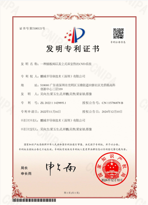
Warm congratulationsPengcheng SemiconductorA Plug Valve and Vertical Double Chamber Hot Wire CVD System》 invention patent has been authorized by the National Intellectual Property Administration and will receive the national invention patent certificate on December 10, 2024.

In the wave of technological innovation, Pengcheng Semiconductor once again won the honor of the national invention patent certificate with its outstanding R&D strength and profound technical accumulation.

This milestone achievement is not only a strong proof of Pengcheng Semiconductor's technological innovation capabilities but also a brilliant crystallization of its deep cultivation and continuous exploration in the semiconductor field. The invention patent for the plug valve and vertical double chamber hot wire CVD system not only signifies a major breakthrough in high-end equipment manufacturing technology for Pengcheng Semiconductor but also indicates that the company has taken solid steps in improving the efficiency and quality of semiconductor material preparation. The acquisition of this patent will lay a solid foundation for the company to further expand domestic and international markets and deepen cooperation with upstream and downstream enterprises in the industry chain, while also contributing valuable strength to China's semiconductor industry's independent controllability and high-quality development. Pengcheng Semiconductor will continue to uphold the spirit of innovation, committed to more core technology research and breakthroughs, contributing to the vigorous development of China's semiconductor industry.


News Center

The global MBE market is steadily growing, with China's Pengcheng Semiconductor breaking through technological monopolies

In 2021, the global market size of Molecular Beam Epitaxy (MBE) systems was approximately 550 million RMB. Looking ahead to 2028, this figure is projected to climb to 960 million RMB, signifying a consistent expansion of the market at a compound annual growth rate (CAGR) of 8.3% between 2022 and 2028. MBE systems play a crucial role in semiconductor and basic materials research. Major consumers include countries with well-established industrial systems such as Europe, the United States, Japan, and China, which collectively account for over 80% of the global market share.

Forwarding Science and Technology News | Enriching Forms to Promote Services, Accurate Services to Promote Innovation

May 15, 2025, marks the 19th annual "Government Affairs Open Day" in the province. Centering on the theme of "Deepening Government Affairs Openness to Support the Decisive Battle and Victory," the Shenyang Municipal Science and Technology Innovation Service Center leveraged this opportunity, combining publicity of Shenyang's science and technology innovation policies with the needs of assisting enterprises, to conduct a special research and visit activity. This research focused on Pengcheng Micronanotechnology (Shenyang) Co., Ltd., aiming to publicize the achievements in the construction of Shenyang's science and technology innovation platforms, the sharing of resources from science and technology infrastructure platforms, and the results of the implementation of innovation voucher policies. The goal is to promote the collaborative development of the Shenyang Municipal Science and Technology Intermediary Service Alliance, further optimize the business environment, and support enterprise innovation breakthroughs.

Thin film deposition equipment

Thin film deposition equipment classification Thin film deposition refers to the deposition of thin film materials to be processed on substrates such as silicon wafers. The deposited thin film materials are mainly non-metals such as silicon dioxide, silicon nitride, and polysilicon, as well as metals such as copper. The deposited films can be amorphous, polycrystalline, or single crystal.

Exhibition Invitation | Pengcheng Semiconductor sincerely invites you to attend the 7th Global Semiconductor Industry (Chongqing) Expo

The 7th Global Semiconductor Industry (Chongqing) Expo will be held at the Chongqing International Expo Center from May 8th to 10th, 2025. Themed "New Era • Creating a Smart Future", the expo will cover 40,000 square meters, feature 800 exhibitors, and attract 35,000 professional visitors.

Pengcheng Semiconductor has been awarded the title of National High-tech Enterprise, leading a new journey in nano and atomic manufacturing technology.

In the current era of rapid technological development, the semiconductor industry, as the cornerstone of modern information technology, is continuously driving innovation and transformation in various fields. Recently, Pengcheng Semiconductor Technology (Shenzhen) Co., Ltd. successfully obtained the national high-tech enterprise certification due to its outstanding technological innovation capabilities and significant contributions in the semiconductor field. This honor is not only a high recognition of Pengcheng Semiconductor's past efforts but also marks the authoritative certification of its leading position in the field of nano and atomic manufacturing technology.