

Hot filament chemical vapor deposition (HFCVD) diamond coating equipment manufacturers "seismic information"
Release time:
2024-07-22


As an ultra-wide bandgap semiconductor material, diamond has excellent physical properties such as high carrier mobility, high thermal conductivity, high breakdown electric field, high carrier saturation rate and low dielectric constant, and is considered to be the "ultimate semiconductor" for the preparation of the next generation of high power, high frequency, high temperature and low power loss electronic devices ".
Compared with advanced countries, China's diamond semiconductor industry exists: 1, the key equipment depends on imports, no independent intellectual property rights, vulnerable to foreign blockade; 2, the lack of large-size diamond substrate preparation and thin film epitaxial growth process; 3, diamond grinding, bonding, thinning technology is not mature and other gaps. This project brings together top scientific research teams in universities and excellent engineers in industry to open up the research and development and production links required for industrialization, such as high-quality diamond film growth, HFCVD hot wire CVD diamond equipment customization, wafer grinding and bonding thinning, etc. It starts from tool-level and thermal-level products, and will continue to promote the research and development of optical-level, electronic-level and even quantum-level products.
Pengcheng Semiconductor Technology (Shenzhen) Co., Ltd. (hereinafter referred to as: Pengcheng Semiconductor) independently developed HFCVD hot filament chemical vapor deposition equipment (hot filament chemical vapor deposition (HFCVD) diamond coating equipment) can be used for the production of micron crystal and nanocrystalline diamond wafers, as well as anti-corrosion and wear-resistant hard coatings, diamond BDD electrodes, solar thin film batteries, etc.
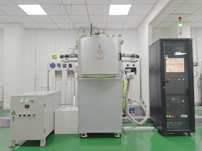
Independent research and development and production of single/double coated hot filament CVD diamond equipment (HFCVD) can prepare diamond polycrystalline wafer substrate size: 2 inches, 4 inches, 6 inches, 8 inches.
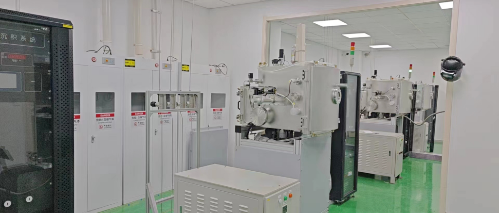
Diamond film production line
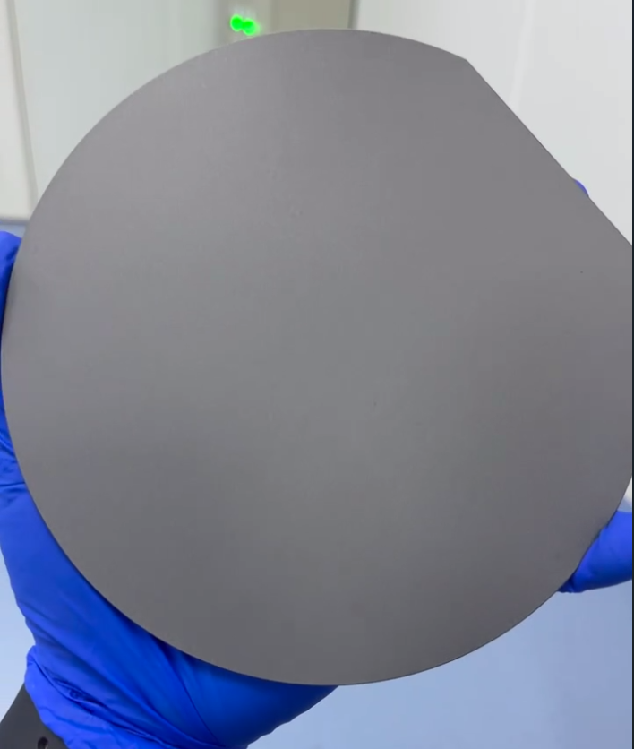

6 inch diamond cooling wafer
Application areas: third-generation semiconductors, high-power lasers, 10G communications, micro-nano acoustics, power amplifiers, filter devices, etc.; can be used for the development and production of diamond products of mechanical, thermal, optical and acoustic levels.
Company Profile:
Pengcheng Semiconductor Technology (Shenzhen) Co., Ltd. was jointly initiated by Harbin Institute of Technology (Shenzhen) and a team of engineers with many years of practical experience. Based on the intersection of market frontier, industry frontier and technology frontier, the company seeks innovation guidance and sustainable development, solves the pain points of the industry and the problem of localization, and strives for the independent control of the industrial chain.
The company's core business is micro-nano materials (including semiconductor materials), micro-nano manufacturing process, micro-nano equipment research and development design and manufacturing.
Scientific research equipment: PVD, CVD, MBE molecular beam epitaxy, etc.
Industrial production equipment: large-scale evaporation equipment, multi-arc ion source coating equipment, rectangular magnetron sputtering coating equipment, electron beam evaporation equipment, OLED coating equipment, HFCVD hot wire chemical vapor deposition equipment, vacuum high temperature CVD furnace, six-inch MBE production equipment.
The company's technology and products can be widely used in: new materials, new energy, microelectronics, optoelectronics, semiconductors, acoustics, optics, micro-electromechanical systems (MEMS); sensors, biomedicine, precision medicine, health, environmental protection, micro-nano robots, Surface technology and other fields.
The company's core R & D team has a complete knowledge structure, including a high-level material research and process research team with professors and doctors of Harbin Institute of Technology as the core, as well as a team of senior equipment designers from the industry. The company team has more than 20 years of experience in micro-nano materials and device research (including semiconductor materials), PVD/CVD deposition technology research, epitaxial technology research, thin film preparation equipment design and manufacturing.

News Center
“The Coating Black Technology” Hidden in Medical Imaging

Contact: Miss Dai
Address: 1704, Building 1, Chongwen Park, Nanshan Zhiyuan, 3370 Liuxian Avenue, Nanshan District, Shenzhen City, Guangdong Province
Shenyang Office Address: Shenyang University Science Park, No.15 Wanghua South Street, Dadong District, Shenyang City, Liaoning Province
Telephone:13632750017
E-mail:sales@hitsemi.com

Message