

Pengcheng Semiconductor HFCVD hot filament chemical vapor deposition equipment cost-effective manufacturer "Typhoon Express"
Release time:
2024-07-09


Diamond is a typical multi-functional limit material, which has excellent properties in electrical, optical, thermal, mechanical acoustics and electrochemistry, and has broad application prospects in many high-tech fields.
After the 1980 s, the preparation of diamond coatings by chemical vapor deposition (CVD) technology promoted its wide application and triggered the "diamond heat" that swept the world ". After the 1990 s, with the emergence of industrialized diamond coating preparation technology, the diamond coating industry began to sprout. A series of high-tech value-added products such as diamond coated tools, diamond heat sinks, diamond optical windows, diamond film-based detectors and sensors, and diamond electrodes have begun to enter the market, which has greatly promoted precision machining, biomedicine, electrochemistry, sensing and Industrial upgrading in the fields of detection and semiconductors.
At the beginning of the 21st century, CVD diamond industry began to appear in China. At present, it mainly covers carbide-based diamond coated tools and molds, tool-grade, heat sink-grade and optical-grade diamond self-supporting films, and shows a good momentum of development. Moreover, China's diamond coating research has been highly concerned by the country. The National "863" Program and the National Natural Science Foundation of China have continued to fund related research projects. During the "Eighth Five-Year Plan", "Ninth Five-Year Plan" and "Eleventh Five-Year Plan", major key technology projects and special projects for key materials have been set up around diamond coatings, and significant results have been achieved.
Pengcheng Semiconductor Technology (Shenzhen) Co., Ltd. (hereinafter referred to as: Pengcheng Semiconductor) independent research and development of HFCVD hot filament chemical vapor deposition equipment can be used for micron crystal, nanocrystalline diamond wafer production, can also be made of anti-corrosion wear-resistant hard coating, diamond BDD electrode, solar thin film cells.
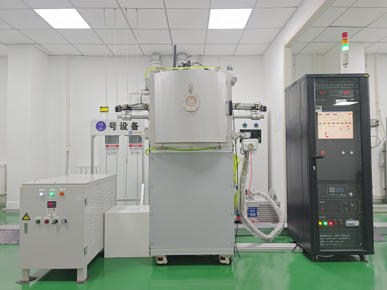
Independent research and development and production of single/double coated hot filament CVD diamond equipment (HFCVD) can prepare diamond polycrystalline wafer substrate size: 2 inches, 4 inches, 6 inches, 8 inches.

Diamond film production line
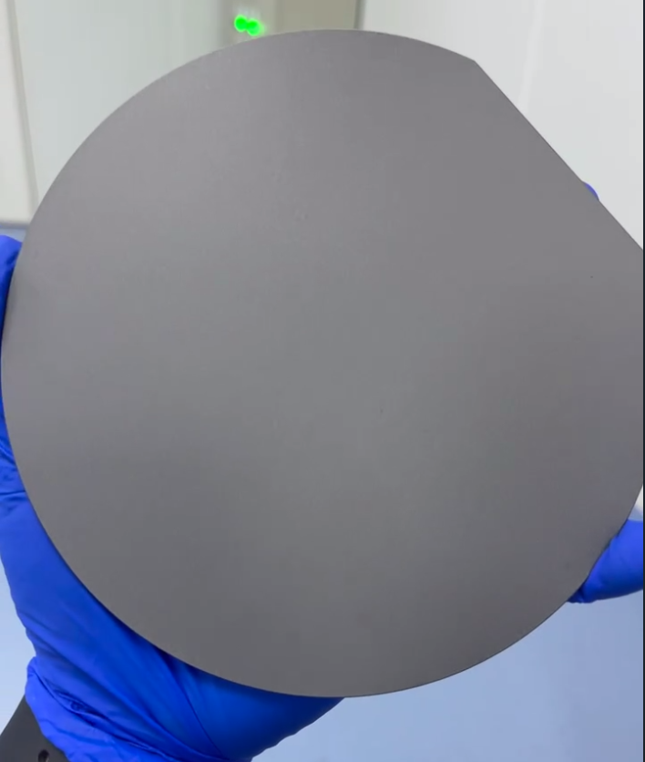
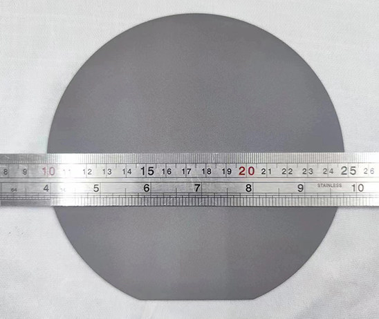
6 inch diamond cooling wafer
Application areas: third-generation semiconductors, high-power lasers, 10G communications, micro-nano acoustics, power amplifiers, filter devices, etc.; can be used for the development and production of diamond products of mechanical, thermal, optical and acoustic levels.
Company Profile:
Pengcheng Semiconductor Technology (Shenzhen) Co., Ltd. was jointly initiated by Harbin Institute of Technology (Shenzhen) and a team of engineers with many years of practical experience. Based on the intersection of market frontier, industry frontier and technology frontier, the company seeks innovation guidance and sustainable development, solves the pain points of the industry and the problem of localization, and strives for the independent control of the industrial chain.
The company's core business is micro-nano materials (including semiconductor materials), micro-nano manufacturing process, micro-nano equipment research and development design and manufacturing.
Scientific research equipment: PVD, CVD, MBE molecular beam epitaxy, etc.
Industrial production equipment: large-scale evaporation equipment, multi-arc ion source coating equipment, rectangular magnetron sputtering coating equipment, electron beam evaporation equipment, OLED coating equipment, HFCVD hot wire chemical vapor deposition equipment, vacuum high temperature CVD furnace, six-inch MBE production equipment.
The company's technology and products can be widely used in: new materials, new energy, microelectronics, optoelectronics, semiconductors, acoustics, optics, micro-electromechanical systems (MEMS); sensors, biomedicine, precision medicine, health, environmental protection, micro-nano robots, Surface technology and other fields.
The company's core R & D team has a complete knowledge structure, including a high-level material research and process research team with professors and doctors of Harbin Institute of Technology as the core, as well as a team of senior equipment designers from the industry. The company team has more than 20 years of experience in micro-nano materials and device research (including semiconductor materials), PVD/CVD deposition technology research, epitaxial technology research, thin film preparation equipment design and manufacturing.

News Center
Application of TGV Glass Through-Hole Technology in Magnetron Sputtering
Pengcheng Semiconductor: The Strategy, Tactics, and Survival Guide of a High-Tech Enterprise

Contact: Miss Dai
Address: 1704, Building 1, Chongwen Park, Nanshan Zhiyuan, 3370 Liuxian Avenue, Nanshan District, Shenzhen City, Guangdong Province
Shenyang Office Address: Shenyang University Science Park, No.15 Wanghua South Street, Dadong District, Shenyang City, Liaoning Province
Telephone:13632750017
E-mail:sales@hitsemi.com

Message