

Application of PVD Technology in Semiconductor Devices
Release time:
2024-07-04


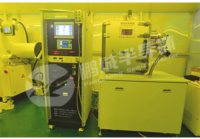
In the rapidly developing field of semiconductor technology, physical vapor deposition (PVD) is a key tool to achieve the accuracy and efficiency of thin film deposition processes. Let's take a look at the advanced applications of PVD technology in the semiconductor industry.
Physical vapor deposition involves depositing a thin film on a semiconductor substrate using a physical process such as sputtering or evaporation. The versatility and controllability of PVD make it a valuable tool in semiconductor manufacturing, enabling the creation of complex and high-performance devices.
Application of PVD in Advanced Microelectronics
Thin film transistors (TFTs)
PVD plays a key role in the manufacture of TFTs, which are the basic components of flat panel displays, organic light emitting diodes (OLEDs) and other emerging display technologies. PVD technology improves the performance of TFTs, improves response time, and reduces power consumption, making a significant contribution to the development of display technology.
Interconnect and Metallization
As semiconductor devices become more compact, efficient interconnects become critical. PVD helps create reliable metal interconnects with minimal resistivity, improving signal speed and device reliability. The case study will clarify the key role of PVD in advanced metallization processes to ensure optimal device performance.
Semiconductor Packaging
PVD plays an important role in the production of protective coatings for semiconductor devices, protecting them from environmental factors and ensuring longevity. We will delve into how PVD can help create a protective layer that improves the durability and reliability of equipment, especially in challenging operating environments.
The implementation of physical vapor deposition (PVD) in the manufacture of logic and memory devices has revolutionized semiconductor memory technology.
Here are some application scenarios that demonstrate the important role of PVD in the field.
High-density memory storage
In the field of high-density memory storage, PVD technology has played an important role in pushing the boundaries of data storage capabilities. Case studies reveal examples of PVD used to deposit thin films with exceptional precision, enabling the creation of densely packed storage cells. This can not only maximize the storage capacity, but also improve the data retrieval speed, thereby improving the efficiency of the storage device.
Logic Circuit Performance Enhancement
Logic circuits are the backbone of semiconductor devices, and PVD plays a key role in improving their performance. By controlling the deposition process, PVD ensures the creation of high-quality interconnects and metal layers, reduces resistivity and improves signal propagation. The case study highlights how PVD can help manufacture logic circuits with superior speed, reliability, and energy efficiency.
The accuracy and reliability provided by PVD technology is a key factor in the continuous advancement of semiconductor memory technology, pushing the achievable boundaries in terms of storage capacity and processing speed.
PVD for advanced sensor technology
The application of physical vapor deposition (PVD) in the development of advanced sensor technologies has far-reaching implications in various fields such as automotive, healthcare, and consumer electronics. Here are some illustrative examples that highlight the key role of PVD in this area.
1. Automotive sensors
In the automotive industry, sensors are an important part of various applications, including safety systems and engine management. PVD is used to form a thin film on the sensor surface to improve sensitivity and response time. Real-world examples demonstrate how PVD can help improve the accuracy of automotive sensors, enabling advances in driver assistance systems and overall vehicle safety.

2. Medical sensors
PVD plays an important role in the development of sensors used in healthcare applications such as medical imaging devices and diagnostic tools. Through a precise deposition process, PVD ensures the creation of the sensor coating, improving sensitivity and biocompatibility. The case study demonstrates how PVD can help produce reliable and accurate healthcare sensors, ultimately improving patient care and diagnostic capabilities.

3. Consumer Electronics Sensors
From touch screens to motion sensors, consumer electronics rely on sensors for a variety of functions. PVD technology is used to create a protective and conductive layer on the sensor surface to improve durability and responsiveness. Examples highlight how PVD can enhance the reliability of sensors in consumer electronics, contributing to the seamless and efficient operation of equipment.

Conclusion
As semiconductor devices continue to evolve in complexity and functionality, the role of PVD in their fabrication becomes increasingly important. This article provides a comprehensive overview of the advanced applications of PVD technology in the semiconductor industry. The versatility of PVD opens up new possibilities for innovation and ensures that the semiconductor industry is always at the forefront of technological progress.
News Center

Contact: Miss Dai
Address: 1704, Building 1, Chongwen Park, Nanshan Zhiyuan, 3370 Liuxian Avenue, Nanshan District, Shenzhen City, Guangdong Province
Shenyang Office Address: Shenyang University Science Park, No.15 Wanghua South Street, Dadong District, Shenyang City, Liaoning Province
Telephone:13632750017
E-mail:sales@hitsemi.com

Message